AMD's RDNA 2 Gets A Codename: “Navi 2X” Comes This Year With 50% Improved Perf-Per-Watt
by Ryan Smith on March 5, 2020 5:45 PM EST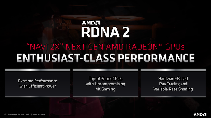
While AMD’s Financial Analyst Day is first and foremost focused on the company’s financial performance – it’s right there in the title – this doesn’t stop the company from dropping a nugget or two of technical information along the way, to help excite investors on the future of the company.
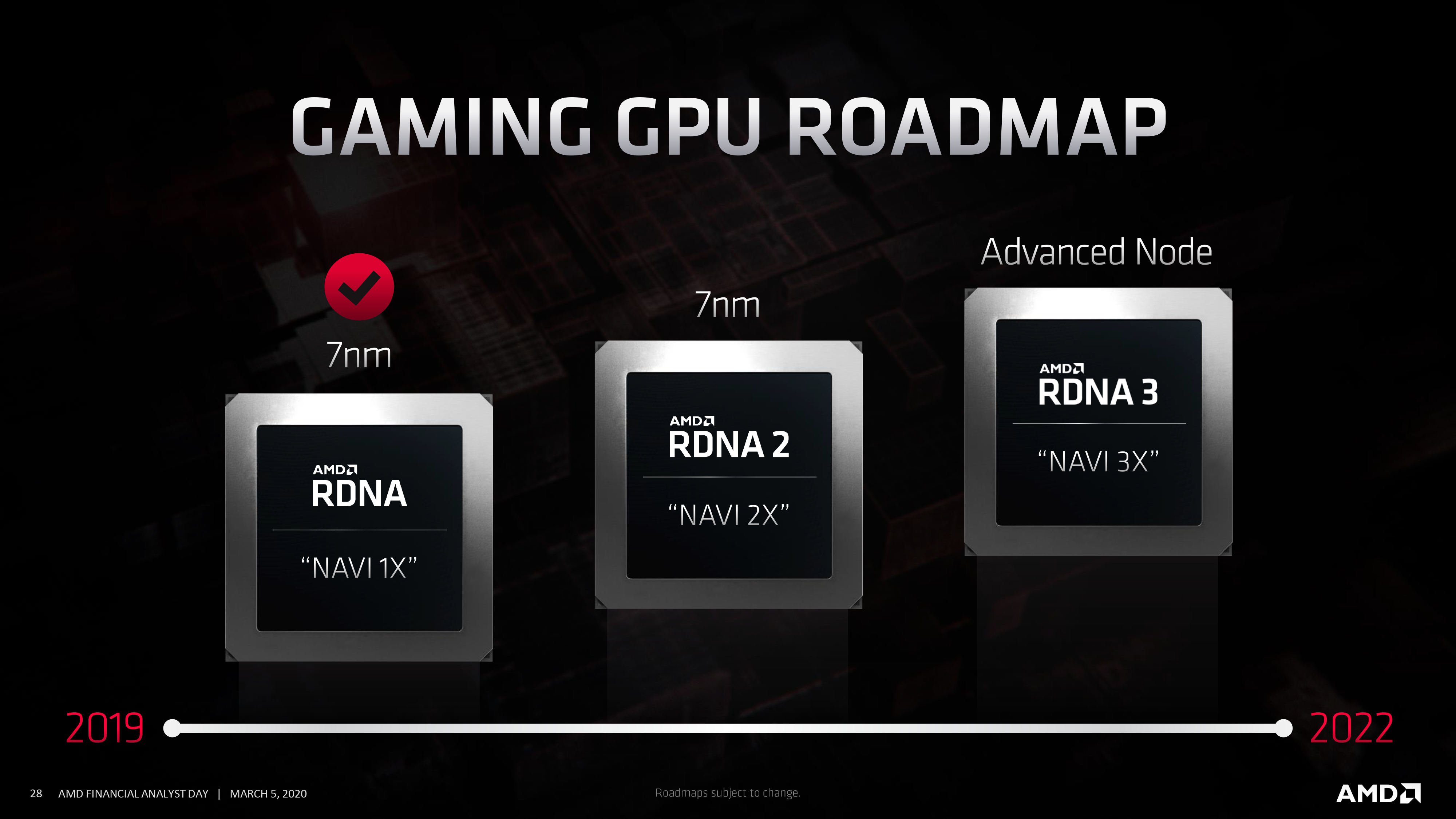
One such nugget this year involves AMD’s forthcoming RDNA 2 family of client GPUs. The successor to the current RDNA (1) “Navi” family, RDNA 2 has been on AMD’s roadmap since last year. And it’s been previously revealed that, among other things, it will be the GPU architecture used in Microsoft’s forthcoming Xbox Series X gaming console. And while we’re still some time off from a full architecture reveal from AMD, the company is offering just a few more details on the architecture.
First and foremost, RDNA 2 is when AMD will fill out the rest of its consumer product stack, with their eye firmly on (finally) addressing the high-end, extreme performance segment of the market. The extreme high end of the market is small in volume, but it’s impossible to overstate how important it is to be seen there – to be seen as competing with the best of the best from other GPU vendors. While AMD isn’t talking about specific SKUs or performance metrics at this time, RDNA 2 will include GPUs that address this portion of the market, with AMD aiming for the performance necessary to deliver “uncompromising” 4K gaming.
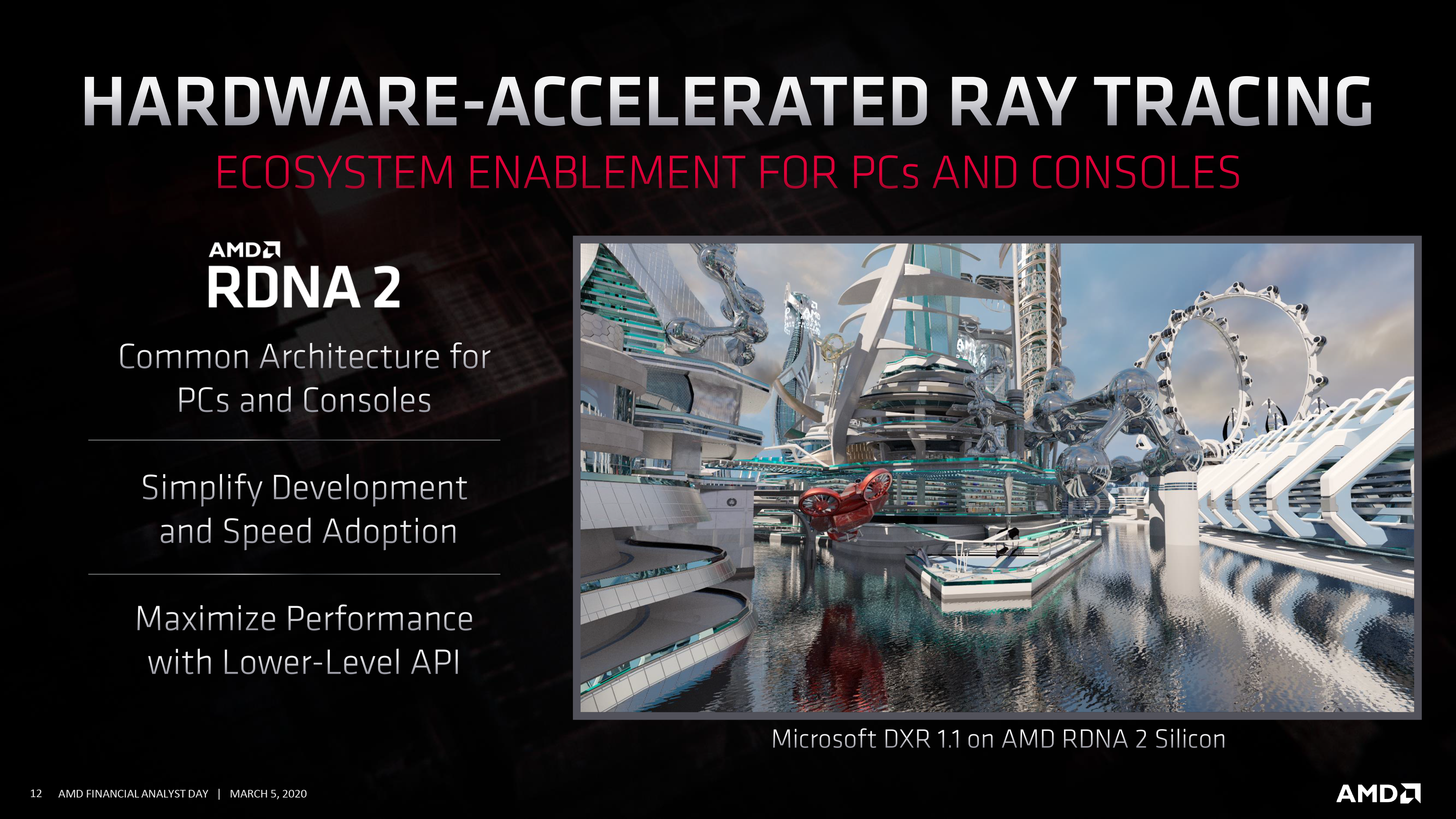
But don’t call it "Big Navi". RDNA 2 isn’t just a series of bigger-than-RDNA (1) chips. The GPUs, which will be the codename “Navi 2X” family, also incorporate new graphics features that set them apart from earlier products. AMD isn’t being exhaustive here – and indeed they’re largely already confirming what we know from the Xbox Series X announcement – but hardware ray tracing as well as variable rate shading are on tap for RDNA 2. This stands to be important for AMD at multiple levels, not the least of which is closing the current feature gap with arch-rival NVIDIA.
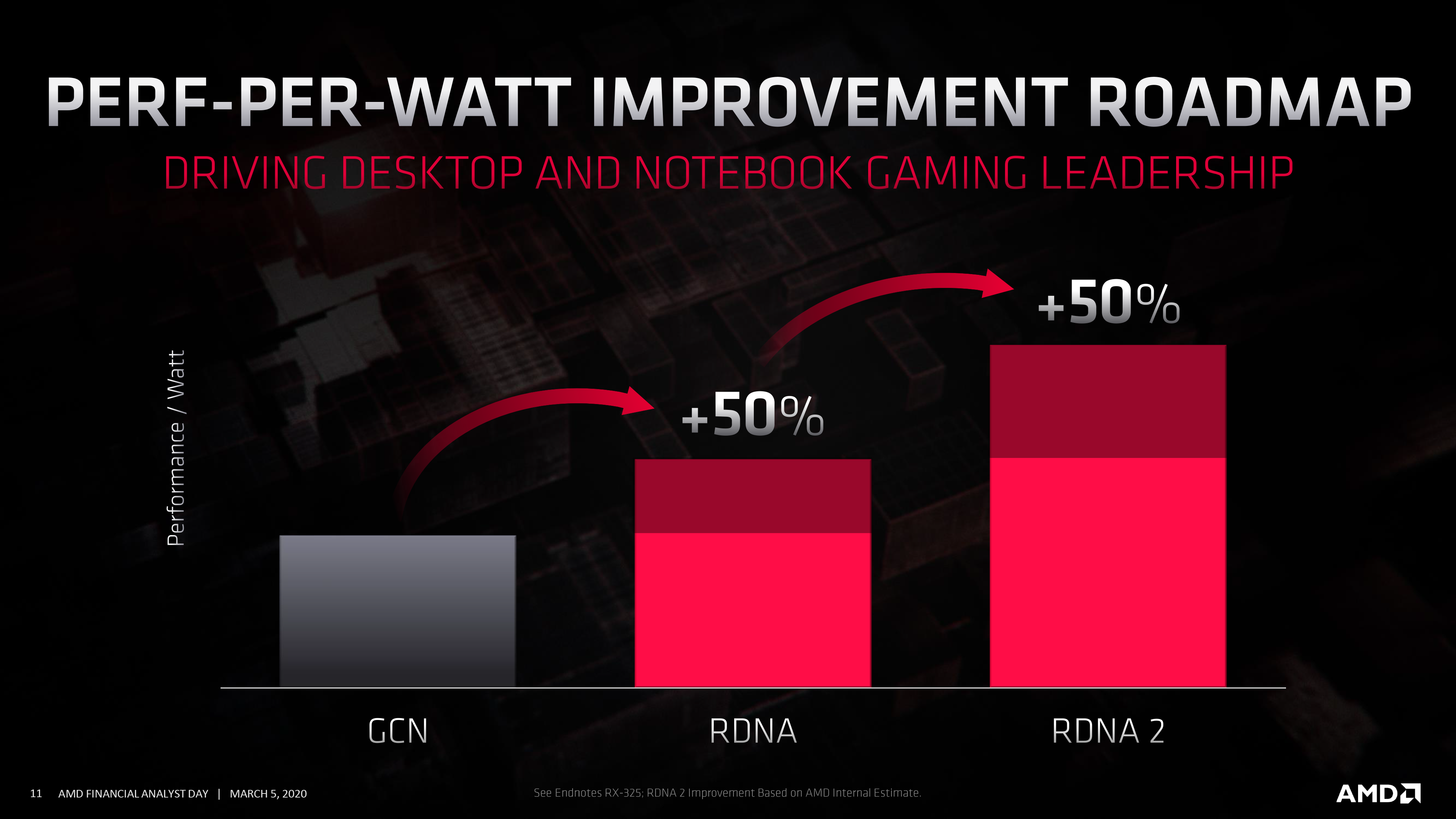
And AMD didn’t stop there, either. Even to my own surprise, AMD isn’t just doing RDNA (1) with more features; RDNA 2 will also deliver on perf-per-watt improvements. All told, AMD is aiming for a 50% increase in perf-per-watt over RDNA (1), which is on par with the improvements that RDNA (1) delivered last year. Again speaking at a high level, these efficiency improvements will come from several areas, including microarchitectural enhancements (AMD even lists improved IPC here), as well as optimizations to physical routing and unspecified logic enhancements to “reduce complexity and switching power.”
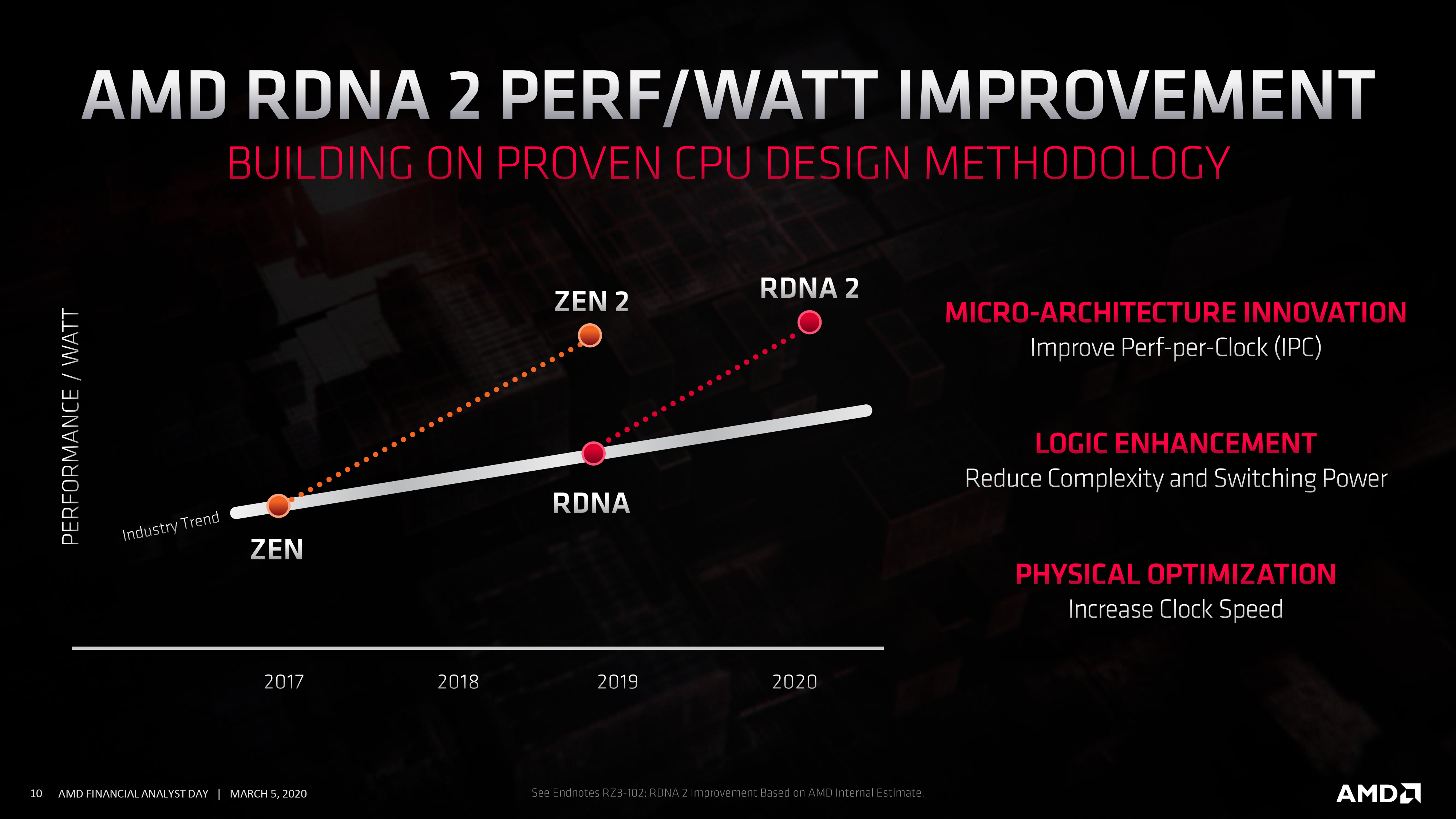
Process nodes will also play some kind of a role here. While AMD is still going to be on a 7nm process here – and they are distancing themselves from saying that they'll be using TSMC’s EUV-based “N7+” node – the company has clarified that they will be using an enhanced version of 7nm. To what extent those enhancements are we aren’t sure (possibly using TSMC’s N7P?), but AMD won’t be standing still on process tech.
This strong focus on perf-per-watt, in turn, will be a key component of how AMD can launch itself back into being a fully viable, top-to-bottom competitor with NVIDIA. While AMD is already generally at parity with NVIDIA here, part of that advantage comes from an atypical advantage in manufacturing nodes that AMD can’t rely on keeping. NVIDIA isn’t standing still for 2020, and neither can AMD. Improving power efficiency for RDNA 2 (and beyond) will be essential for convincingly beating NVIDIA.
Overall, AMD has significant ambitions with RDNA 2, and it shows. The architecture will be the cornerstone of a generation of consoles, and it will be AMD’s first real shot in the last few years at taking back the flagship video card performance crown. So we’re eagerly awaiting to see what else RDNA 2 will bring to the table, and when this year the first video cards based on the new architecture will begin shipping.


46 Comments
View All Comments
sorten - Thursday, March 5, 2020 - link
Whoa, I wasn't even expecting AMD news today. Sounds awesome, and this year even!Thanks for the coverage.
milkywayer - Thursday, March 5, 2020 - link
I wonder if Covid19 is going to impact the ps5 and nexbox launch. I mean it will but wondering how much.Kangal - Friday, March 6, 2020 - link
As far as I know, they won't delay the launch.But it will have an affect on the stock availability, and quantities will remain low for the first 6 months of its lifecycle. The more interesting tidbit is the pricing. We know Microsoft is huge, has cash reserves to take the hit, but not Sony.
Sony was planning on making a $400 console, and sell it for $500. So there's little ($100) to ($0) no profit margin there. However, it seems now the costs have increased to $550. That means they need to take a small ($50) to ($100) medium loss per unit. Or they could sell it for $600, and maintain their minimal profit margin, but that seems unlikely based on sour-history with the PS3 launch.
The ideal scenario is to delay the launch by 6 months, since the PS4 and PS4 Pro are young enough, powerful enough, and popular enough to allow this. Though that won't happen as Sony Executives do not want to miss the Holiday Period, unlike Nintendo which doesn't care. Maybe they can announce the PS5 a week before release, and in the announcement state that its RRP is $499.... but for the first 6-months the consoles will be sold as "Founders Edition" with a premium $600 price. It think that's the best approach.
As long as they do not use these circumstances to downgrade the console, I'm all for it. Since price can change, but hardware specs are locked-in for over 6 years. We have been expecting the console to ship with specs similar to a Midrange Gaming PC: r7-3700X, RX 5700, 32GB RAM (shared GDDR6), and 1TB SSD (or instead a soldered 256GB SSD + 1TB HDD removable).
Crazyeyeskillah - Thursday, March 5, 2020 - link
I've never seen this much extremely specified info dropped at a fin an day.If Big Navi didn't have people's ears pinned, this will certainly get the job done.
8k compute units, with something like 17% ipc gain, increased clocks, and the like - we're looking at a serious powerhouse.
tuxRoller - Thursday, March 5, 2020 - link
Where did you come across these numbers?Novacius - Thursday, March 5, 2020 - link
Your're confusing a lot of information. The 128 CUs/8192 ALUs belong to Arcturus, an HPC-only GPU that is based on an adjusted Vega architecture. And the 17% IPC were a rumor regarding Zen 3.HarryVoyager - Thursday, March 5, 2020 - link
So what I've heard is most likely 80 CU, and if they're able to do that with only about 60% of the power from RDNA1 that should put them within reach of those 40% better than the 2080 TI numbers we saw from that VR benchmark a while back, without requiring three eight pin power connectors.Novacius - Thursday, March 5, 2020 - link
Yeah. 50% better performance per watt would enable a card with 80 CUs/twice the performance of the 5700XT at around 300W.Flunk - Thursday, March 5, 2020 - link
300w TDP would make for a toasty card.Dragonstongue - Thursday, March 5, 2020 - link
depends on FLAT 300w TDP/TBP or "if they are smart" can be "max of" but not will always use. If they take Zen2 into account of the design, 65/105w competing neck and neck with "others" that claim same but in reality chew into the 180+ ACTUAL watt range (when not idling)I always wondered about this, yes bunch of transistors take bunch of power to do their thing, CPU have long been able to "settle down" per ms to not chew power galore, GPU with their many thousands of "small not so smart" shaders (whatever you prefer to call them) have not been able to do this?
seems to me, that is a ripe feature to be targeting eg. loads of performance when you need it, while sipping power when you really do not..Nv managed to do something like this (with use of fancy chip/VREG) for GTX 1xxx generation, not so much for RTX 2xxx, AMD "for the most part" was pretty decent overall in their rated TDP vs actual TDP/TBP ratings, but for some reason have not done much to "harness" power usage when not truly needed, beyond limited user control (through things like afterburner..when you are/were able to use it) to downclock and/or downvolt without forcing a bios flash.
anyways.....
raw 300w, yes sir, that would be a toasty card, thankfully, it is "only" 7nm, vs say if it were 28, 45 etc nm designs, that would make the GTX 480 look like it was a freezer pop (^.^)