10nm
Micron this week officially said that it would equip its fab in Hiroshima, Japan, to produce DRAM chips on its 1γ (1-gamma) process technology, its first node to use extreme ultraviolet lithography, in 2025. The company will be the first chipmaker to use EUV for volume production in Japan and its fabs in Hiroshima and Taiwan will be its first sites to use the upcoming 1γ technology. As the only major DRAM maker that has not adopted extreme ultraviolet lithography, Micron planned to start using it with its 1γ process (its 3rd Generation 10nm-class node) in 2024. But due to PC market slump and its spending cuts, the company had to delay the plan to 2025. Micron's 1γ process technology is set to use EUV...
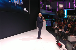
Intel Mentions 10nm, Briefly
LAS VEGAS, NV - Today during a breakfast presentation at CES, Intel's Gregory Bryant, SVP of the Client Computing Group, finally broke Intel's silence on the state of their...
18 by Ian Cutress on 1/9/2018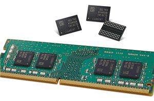
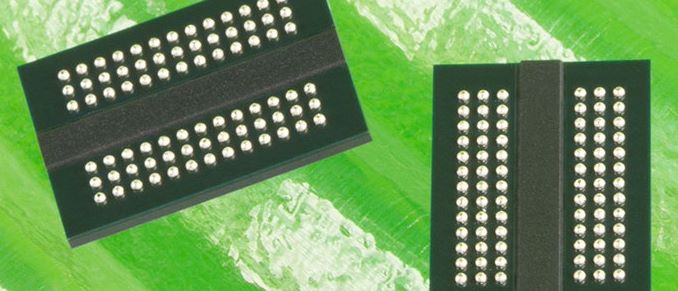
Samsung Starts Production of 8 Gb DDR4-3600 ICs Using 2nd Gen 10nm-Class Tech
Samsung late on Wednesday said that it had initiated mass production of DDR4 memory chips using its second generation '10 nm-class' fabrication process. The new manufacturing technology shrinks die...
24 by Anton Shilov on 12/20/2017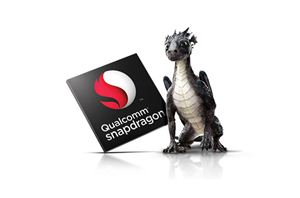
Qualcomm Announces Snapdragon 845 Mobile Platform: Tocks Next-Gen CPU Cores, GPU, AI, & More
Today as part of its media event, Qualcomm finally announced the much expected Snapdragon 845, successor to last year's very successful Snapdragon 835. The Snapdragon 845 is a large...
145 by Andrei Frumusanu on 12/6/2017
Samsung Starts Mass Production of Chips Using 10nm Low Power Plus (10LPP) Process Tech
Samsung Foundry on Wednesday revealed that it has started mass production of SoC products using its second generation 10 nm Low Power Plus (10LPP) fabrication technology. The new manufacturing...
10 by Anton Shilov on 11/29/2017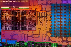
AMD's Progress on Its 25x20 Goal: The Task Ahead
When AMD announced it was creating the new high-performance Zen core, they set a lofty goal. They wanted to produce products that offered 25x the relative efficiency (performance per...
20 by Ian Cutress on 10/26/2017Samsung Details 11LPP Process Technology: 10 nm BEOL Meets 14 nm Elements
Samsung has added a new manufacturing technology into its roadmap. The 11LPP fabrication process is designed for mainstream and higher-end smartphone SoCs. The technology will come online next year...
23 by Anton Shilov on 9/29/2017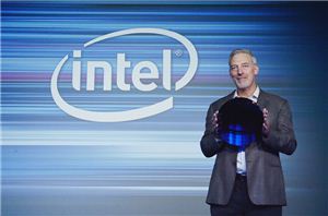
Intel Displays 10nm Wafer, Commits to 10nm ‘Falcon Mesa’ FPGAs
On the back of Intel’s Technology and Manufacturing Day in March, the company presented another iteration of the information at an equivalent event in Beijing this week. Most of...
52 by Ian Cutress on 9/19/2017
Hands on with the LG V30/V30+: 6-inch OLED 2880x1440 Display, Quad DAC, IP68, Daydream VR
As part of their IFA 2017 showcase, this morning LG is unveiling their long-rumored next-generation flagship phone, the V30. Like its predecessor, the LG V20, the V30 hasn't exactly...
125 by Ian Cutress on 8/31/2017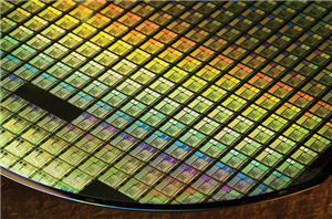
Samsung and TSMC Roadmaps: 8 and 6 nm Added, Looking at 22ULP and 12FFC
Samsung and TSMC have made several important announcements about the present and future of their semiconductor manufacturing technologies in March. Samsung revealed that it had shipped over 70 thousand...
89 by Anton Shilov on 5/5/2017
Samsung Foundry Updates: 7nm EUV, 10LPP, and 14LPC
Earlier this week, Samsung announced a number of updates on the foundry side of their business. While process technology might not be necessarily as interesting as the actual end...
54 by Joshua Ho on 4/22/2016
Intel’s ‘Tick-Tock’ Seemingly Dead, Becomes ‘Process-Architecture-Optimization’
As reported at The Motley Fool, Intel’s latest 10-K / annual report filing would seem to suggest that the ‘Tick-Tock’ strategy of introducing a new lithographic process note in...
98 by Ian Cutress on 3/22/2016
Intel at ISSCC 2015: Reaping the Benefits of 14nm and Going Beyond 10nm
As part of the International Solid-State Circuits Conference every year, Intel brings forward a number of presentations regarding its internal research. The theme this year at ISSCC is ‘Silicon...
55 by Ian Cutress on 2/22/2015


