Chipworks Disassembles Apple's A8 SoC: GX6450, 4MB L3 Cache & More
by Ryan Smith on September 23, 2014 1:00 PM EST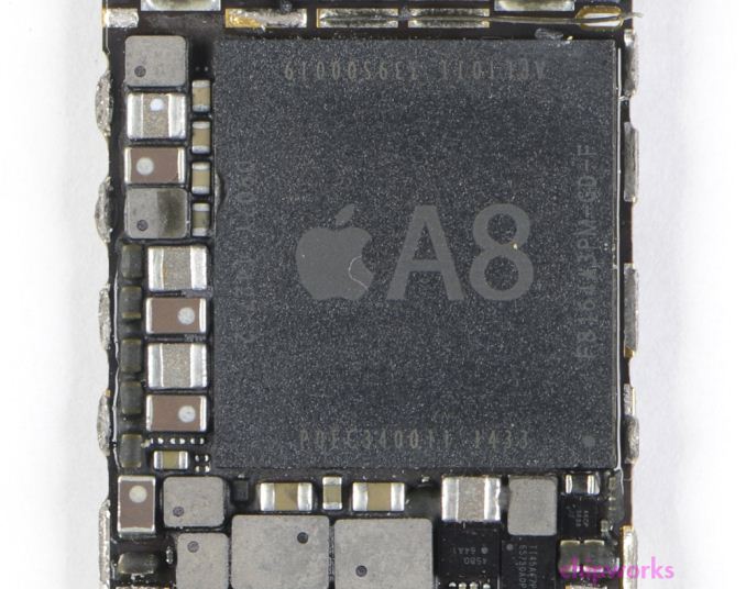
One of the more enjoyable rituals with Apple’s annual iPhone launch is the decapping, deconstruction, and photographing of the processor die at the heart of Apple’s newest SoC. While we can learn a lot about the SoC from software, for some things there’s just no replacement for looking at the hardware itself and counting the functional blocks present. And this year, as in past years, the honor of being the first to tear apart the SoC goes to Chipworks.
For determining the layout of A8, Chipworks reached out to us to solicit our input on their die shot, and after some rounds of going back and forth we believe we’ve come to a solid determination of some of A8’s features and how it has been configured. So let's dive in.
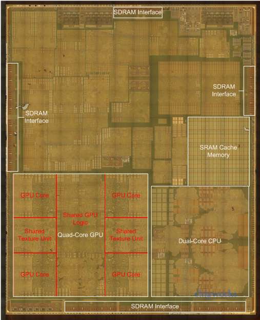
First and foremost we’ll start with A8’s GPU, as this was one of the hardest elements to analyze in software. Based on Apple’s 50% performance improvement we had previously speculated that A8 contained an Imagination PowerVR GX6650. However as we noted back then, a die shot would reveal all, and right on schedule it has.
A close analysis of the die shot makes it clear that there are only 4 GPU cores available and not 6, which immediately rules out the 6 core GX6650 we were previously expecting. Instead with 4 cores present this is conclusive proof that Apple is using the smaller 4 core GX6450 on A8, the direct successor to the G6430 used on the A7. GX6450 induces some performance optimizations along with some feature updates – including ASTC support, which Apple’s documentation has already confirmed is present – so its inclusion here is a natural progression for Apple.
On A8 and its 20nm process this measures at 19.1mm2, versus A7’s 22.1mm2 G6430. As a result Apple is saving some die space compared to A7, but this is being partially offset by the greater complexity of GX6450 and possibly additional SRAM for larger caches on the GPU. Meanwhile looking at the symmetry of the block, it’s interesting that the blocks of texturing resources that every pair of GPU cores share is so visible and so large. With these resources being so big relative to the GPU cores themselves, you can see why Imagination would want to share them as opposed to building them 1:1 with the GPU cores.
Meanwhile opposite the GPU we have the CPU block. Unlike the GPU the CPU block has seen some significant shrinking, which Chipworks estimates is down from 17.1mm2 in A7 to 12.2mm2 in A8. In A7 Cyclone did not lend itself to easily picking apart the individual CPU cores, and neither does the CPU here in A8. We’ll be looking at the new CPU’s architecture in-depth in our iPhone 6 review, but for now it’s safe to say that while this is definitely derived from Cyclone, Apple has added a few tweaks over the last year that make it an even more potent CPU than the first Cyclone. Meanwhile based on this die shot Chipworks believes that the L2 cache has been reorganized to a per-core design, as there is no obvious single block of L2 on A8 like there was A7.
A8 With PoP DRAM Removed
The final major identifiable block on A8 is once again the SRAM cache memory. On A7 we discovered that this block was 4MB and was responsible for servicing the GPU and CPU. On A8 this block is similarly present and serving the same role. This 4MB of SRAM ends up being quite big despite the shrink from 28nm to 20nm, and while at first glance it seems like it should be larger than 4MB given the relative size, in practice what has happened is that the individual SRAM cells have not shrunk by a full 50%. Chipworks estimates the cell size to now be about 0.08µm2, versus 0.12µm2 on A7, which is closer to a 33% shrink that a 50% shrink. As a result the SRAM cache still takes up a fair bit of space, but the value of being able to serve larger memory requests without having to go off-die continues to be immense.
| Apple A8 vs A7 SoCs | ||||
| Apple A8 (2014) | Apple A7 (2013) | |||
| Manufacturing Process | TSMC 20nm HKMG | Samsung 28nm HKMG | ||
| Die Size | 89mm2 | 104mm2 | ||
| Transistor Count | ~2B | "Over 1B" | ||
| CPU | 2 x Apple Enhanced Cyclone ARMv8 64-bit cores | 2 x Apple Cyclone ARMv8 64-bit cores | ||
| GPU | IMG PowerVR GX6450 | IMG PowerVR G6430 | ||
Overall, Chipworks’ analysis points to A8 being fabbed on TSMC’s 20nm process. This makes A8 among the first SoCs to receive the 20nm treatment. Thanks to this smaller node Apple has been able to build in additional features to the SoC while simultaneously shaving off around 15% of their die size. Chipworks estimates the final die size of A8 to stand at 89mm2, versus the 104mm2 for the Samsung 28nm based A7. Chipworks notes that if this were a straight shrink that one would expect the A8 to be closer to 50% the size of A7 (though not all logic can shrink quite that well), which indicates that Apple has spent quite a bit of die size on improving performance through more complex CPU and GPU architectures and miscellaneous feature additions.
Wrapping things up, we’ll be back later this month with our review of the iPhone 6 family and our full analysis of the A8 SoC. So until then stay tuned.

Source: Chipworks


65 Comments
View All Comments
kron123456789 - Tuesday, September 23, 2014 - link
I knew that there is a GX6450 GPU and not GX6650)) But maybe GX6650 will be present in A8X chip, who knows.GC2:CS - Tuesday, September 23, 2014 - link
The main focus was on power efficiency here. Thats why they went with a smaller, lower powered GPU. And you can feel it a lot. Actually it has been said that the A8 is the first Apple A chip that has lower peak power than its predescessor. In battery life test in GFX bench it pushes 38% more pixels on a 16% bigger battery 50% faster and 25% longer than the iPhone 5S. I call that insane... Because even with the same battery cappacity like 5S and same 4,7" display from the 6 it would last somewhat longer.With A7 iPads got a nice battery life bumb. A7 is already very low powered chip for an iPad and A8 is even less so I think it wont be a big impact in battery life, the display is the biggest bottleneck by far in iPad battery life. So efficient in a phone, there is deffinitelly a headroom for improvement in an iPad with "A8X" it could get the G6650 thats about 50% faster as well. It would finally balance the performance (iPads got ~50% more pixels than 1080p 6+) without much battery life impact at all. It would pull about as much power as A7 which isn't a lot at all in an iPad.
We will see if Apple will decide to put in that ultra-efficient iPhone chip like in 2013 or an bumped up chip to utilize platform resources like in 2012.
name99 - Tuesday, September 23, 2014 - link
IF the iPad Pro is real that makes the existence of an A8X even more likely because you then have even more pixels to drive.Of course, another way Apple could handle this is by more aggressive binning --- iPads get 1.5GHz chips, iPad Pro's get 1.6GHz, and Apple considers that good enough --- but that seems like it would not be good enough...
Krysto - Wednesday, September 24, 2014 - link
Except the iPhone 6 Plus uses almost 3x as many pixels as the iPhone 5S/A7 combo. So in fact, the weaker GPU should be LESS efficient for that phone, than a more powerful GPU would've been.akdj - Thursday, September 25, 2014 - link
What 'can't' you do on your iPad? How is it underpowered and finally, how in the WORLD aren't you getting the same battery life I'm getting? 12/14 hours easily, always on. Do a lot of sound and video work and in the field with Lightroom, it's easy to manipulate, correct and upload shots to the base camp in seconds!Sorry. Thought that was a very bizarre comment as an owner of each (still have an original and it's still ten hours away from the wall) & current owner of the second gen minis, an Air and several iPad 4s (we've got a business)
One thing I've NEVER considered was the iPad to be 'underpowered'. I'm floored by its efficiency and abilities to utilize an amazing amount, more than any point in history, of apps/software WITH such power! Photo and video manipulation, music and audio recording and mastering as well, my mini is now me kneeboard providing Jep Charts/Plates ...weather, terrain and traffic in real time, flight planning, filing and 'gas calculator';) ...I guess I've yet to find anything ever on the iPad it couldn't 'handle'. The new MS suite is incredible as are most of the tools/apps provided (gratis) by Apple. iLife and iWork. GarageBand and iMovie instead of Samsung's bloat I've got on my AT&T Note 3 (from both parties, samsung and AT&T).
Anyway, as an iPhone, iPad mini 2 and 5s owner, I can honestly say the 'speed' and 'power', 'efficiency' and yes, battery life are still, four years later a real treat.
That said I'm 43 this weekend and remember my brick Motorola @ work lasting about 100 minutes & my early laptops weighing 12 pounds with a three pound wart that would maybe do an hour and a ½. Today's battery life on these phones, iPads and both our 2012 & 2014 rMBPs.
Have you 'honestly' found software on the iPad that runs slow?
akdj - Thursday, September 25, 2014 - link
Sorry, third to last sentence was supposed to be iPad Air, Mini 2 and 5s. Just to show and reflect on my experiences with the run of A7 devices. Apologies. Still. Need. Edit. :-)subflava - Tuesday, September 23, 2014 - link
So how long will it be before Apple (and other companies will surely follow) starts suing people for disassembling their chips and divulging all their proprietary IP?designerfx - Tuesday, September 23, 2014 - link
never?They don't own images other people generate of a chip's die.
barleyguy - Tuesday, September 23, 2014 - link
That would be like car manufacturers suing people for taking the engine apart...Fergy - Wednesday, September 24, 2014 - link
Stop putting everything in a car metaphor. Cars are constantly copied and nobody is suing each other. In the phone industry they want to own everything and you may copy nothing.