Applied Materials Outlines Next-Gen Tools for 3nm and GAA Transistor Era
by Anton Shilov on May 12, 2022 5:30 PM EST- Posted in
- Semiconductors
- Samsung
- Samsung Foundry
- 3nm
- Applied Materials
- 3GAE
- 3GAP

Last month Samsung Foundry quietly announced that it was set to begin producing chips using its 3GAE (3 nm-class, gate-all-around transistors, early) process technology in the second quarter. While the industry's first 3 nm-class node with GAA transistors is a noteworthy achievement by itself, one thing that is particularly important is that to make GAA transistors efficiently, fabs have to be equipped with new production tools. Fittingly, Applied Materials has recently outlined their next generation of tools that will be used to enable Samsung (and other fabs) to build their first GAA chips.
UPDATE 6/10: Rearranging the order of the text in the Applied Materials section to better reflect the order of GAA fabrication.
Gate-All-Around Transistors: Solving Many Problems at Once
New process technologies should enable higher performance, lower power, and higher transistor density to meet requirements of chip designers. But this combination has been particularly hard to achieve in the recent years as shrinking transistor sizes lead to negative effects like leakage current. To keep scaling performance and voltages while minimizing transistor sizes, the industry began transition from planar to FinFET transistors (which increased the contact area between the channel of the transistor and the gate by making the gate taller) in 2012 and this type of transistors will stay with us for a long time. But the pace of FinFET-based nodes innovation is slowing down as negative aspects of transistors shrinking starting to kick in.
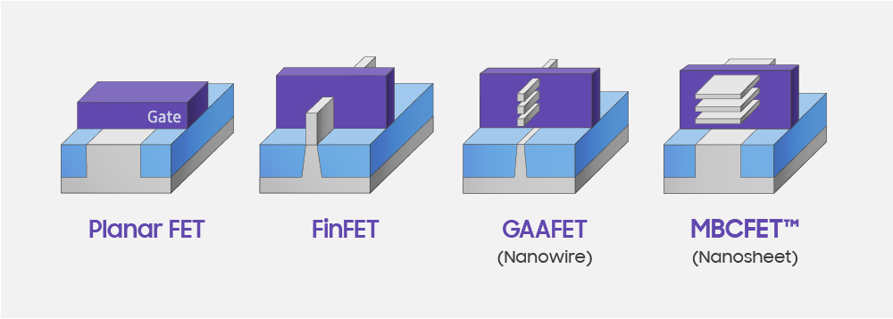
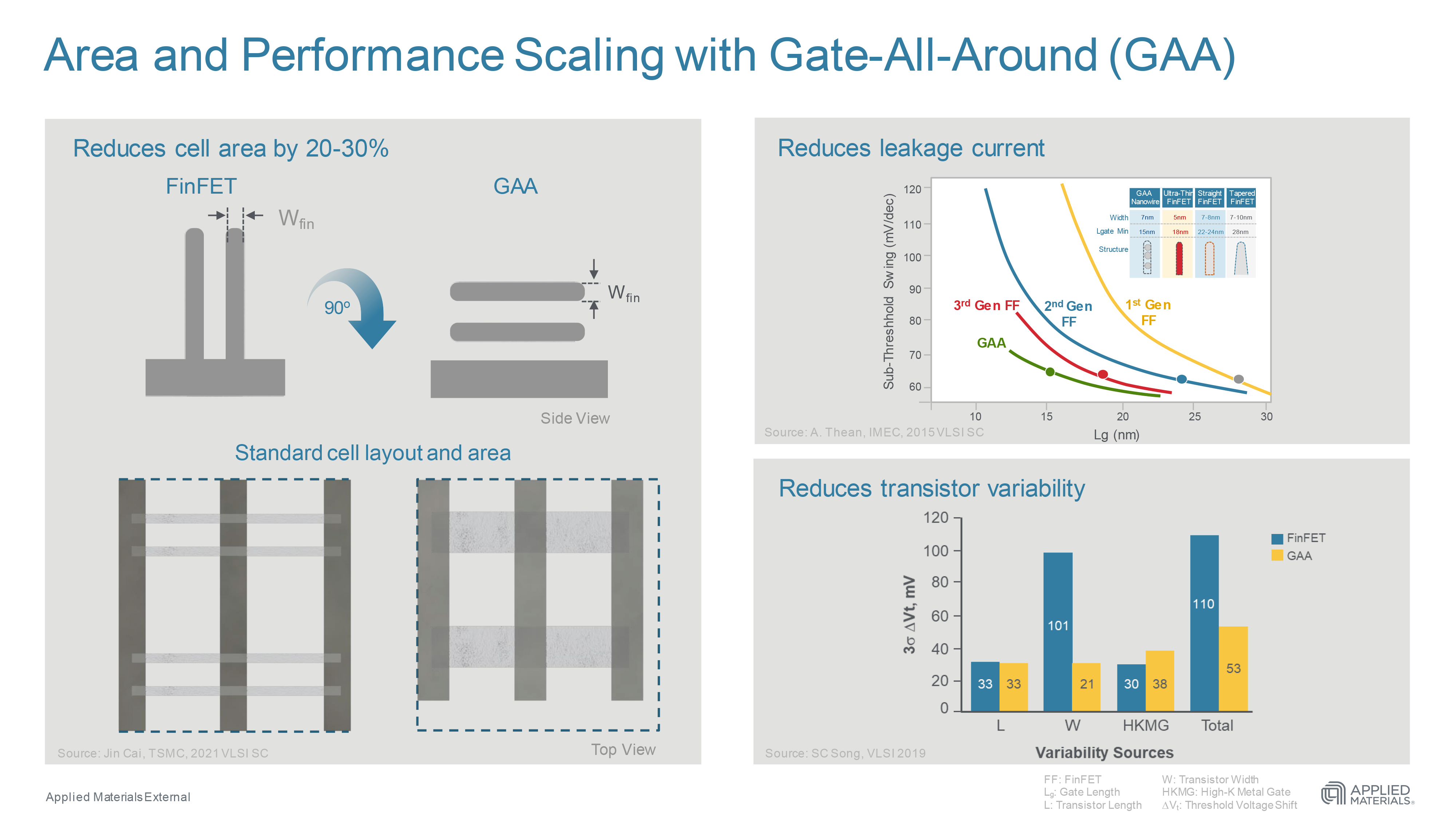
Ever since Intel introduced its 22 nm FinFET-based technology over a decade ago, chipmakers began to talk about the next inevitable step in transistor design, which is gate-all-around. As the name suggests, in GAAFETs channels are horizontal and are surrounded by gates around all four sides of the channels, which solves many problems associated with the leakage current. But this is not the only advantage: in nanosheet/nanoribbon-based GAAFETs it is possible to adjust channel width to get higher performance or reduce power consumption. Since Samsung's 3GAE and 3GAP technologies use nanosheets, Samsung calls its GAAFETs multi-bridge channel field-effect transistors (MBCFETs) to emphasize that it does not use nanowires. Furthermore, Applied Materials claims that GAA architecture reduces transistor variability, which means improved yields and faster time-to-yield (at least as far as transistor performance is concerned) and reduces cell area by 20% to 30%.
While all chipmakers have been talking about GAAFETs and their advantages over FinFETs at various academia industry events, Samsung was the first company to announce a transition to the new type of transistors with its 4 nm node sometimes in 2022 ~ 2023. Eventually, the company's plans changed a bit and in 2019 it unveiled its GAAFET-based 3GAE and 3GAP nodes with high volume manufacturing due in 2022 and 2023, respectively. Last year the company re-emphasized plans to kick off production using its 3GAE in 2022 and this quarter it said that volume production was set to start in Q2.
But Manufacturing Is Challenging
But production of chips using any leading-edge process technology is challenging and making products using Samsung's MBCFET-based 3GAE node certainly poses some risks not only because we are talking about a 3 nm-class manufacturing process, but because manufacturing of GAA transistors is different than making FinFETs.
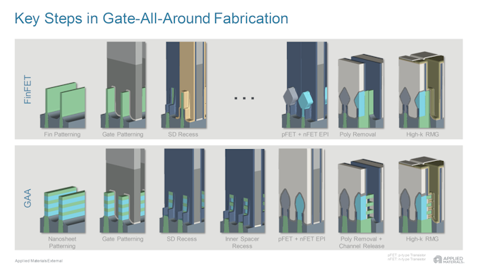
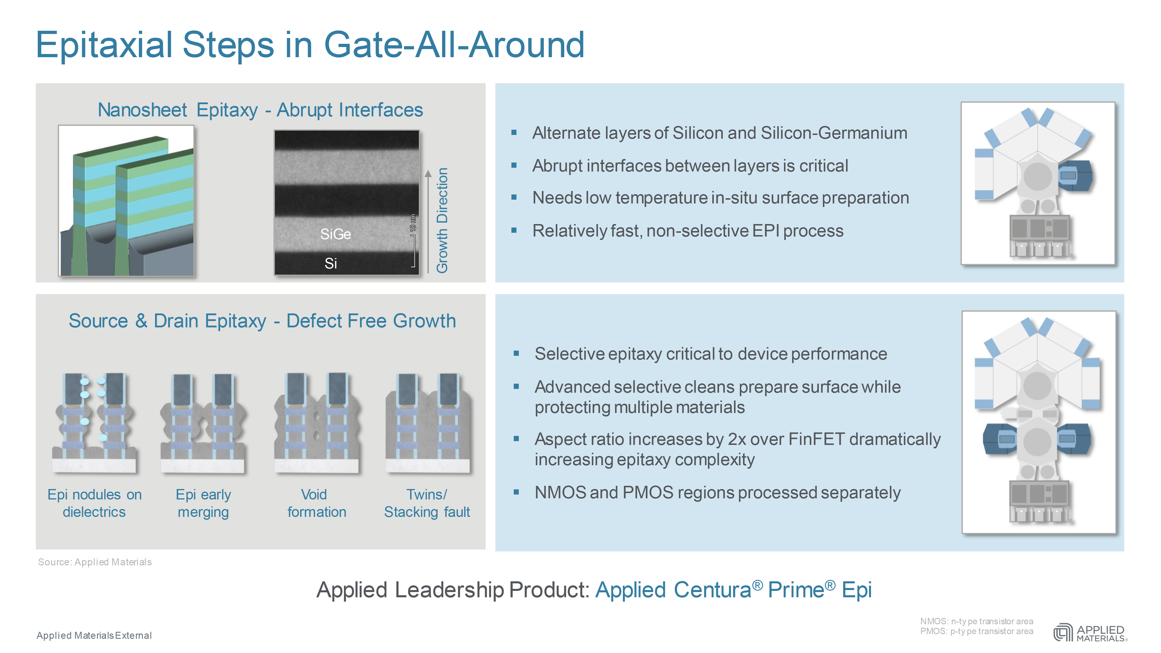
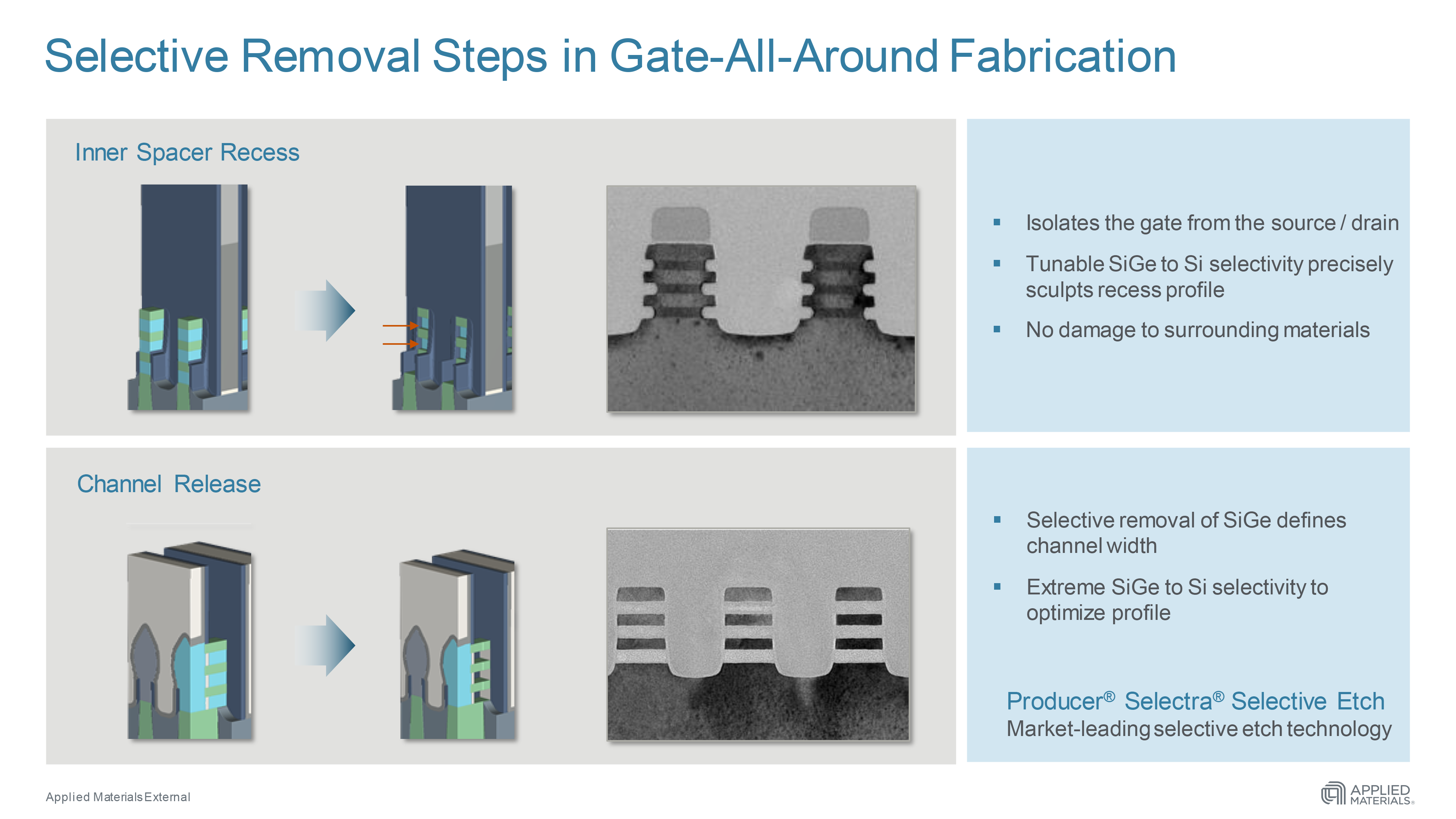
Channels of GAA transistors are shaped using lithography, epitaxy and selective materials removal, processes that enable chipmakers to fine-tune width and uniformity for optimum power and performance. Those selective materials removal and epitaxial steps are considerably more complex when compared to those with FinFETs.
Applied's Producer Selectra Selective Etch IMS tool removes unnecessary SiGe to isolate the gate from the source/drain and define channel width without damaging surrounding materials. Applied introduced its first Selectra etching system in 2016 and since then has shipped over 1,000 chambers that are currently in use by its customers, so the industry is quite aware how to use them. While etching is a widely used process, its usage and importance will grow as the industry begins to transit to newer process technologies, including those based on GAA transistors.
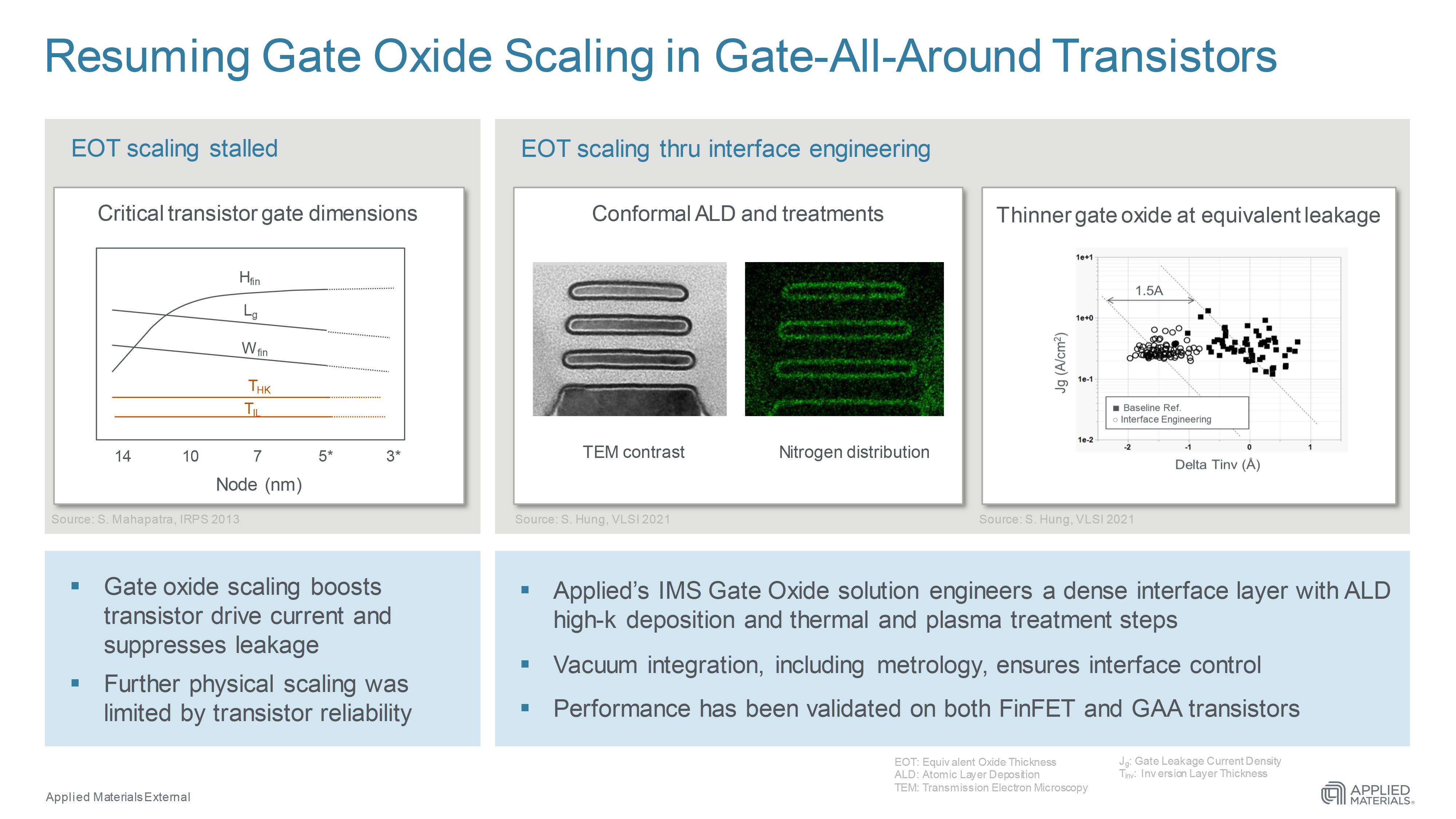
A key challenge with GAAFETs is the need to deposit the multi-layer gate oxide and metal gate stacks around the tiny 10 nm channels. This is where Applied's high-vacuum Integrated Materials Solution (IMS) systems come into play. The Applied Centura Prime Epi tool is used to deposit the Si and SiGe nanosheets with very clean and clear interfaces. Applied’s IMS system for the gate oxide stack integrates atomic layer deposition (ALD), thermal steps, plasma treatment steps, and metrology. Applied's IMS can reduce equivalent gate oxide thickness by 1.5 angstroms, enabling designers to increase performance with no increase in gate leakage or keep performance constant and reduce gate leakage by more than 10 times, the company says.
It is necessary to note that numbers shared by Applied Materials come from various companies (including TSMC, Qualcomm, IMEC, IBM, Intel, and other industry published sources) and should not be applied exclusively to Samsung Foundry's 3GAE and 3GAP nodes. Meanwhile, the general advantages of GAA/MBC/nanoribbon/nanosheet transistors, as well as challenges with their manufacturing, are similar for the whole industry.
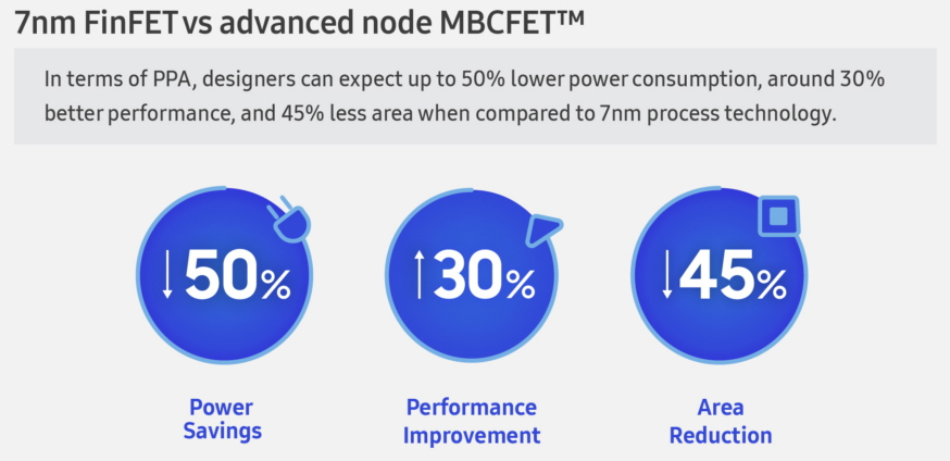
Samsung's 3GAE: +30% Performance, -45% Area
Speaking of advantages, Samsung expects its 3GAE process to offer a 30% performance increase or a 50% power consumption reduction, and a 45% area reduction when compared to 7LPP. Such tangible benefits may be enough to justify challenges associated with this transition in the short term.
For now, the use of 3GAE manufacturing technology that relies a brand-new transistor structure is challenging in general, as in addition to new electronic design automation (EDA) tools, Samsung will need to invent new IP, and adopt brand-new design rules. All of these things, when combined with new lithography, new etching, and new deposit steps are going to make Samsung's transition difficult.
But in exchange, it will start gaining experience with GAA transistors years ahead of Intel and TSMC, which may bring certain gains in the long-term future. Furthermore, experience with GAAFETs will be beneficial for Samsung's DRAM manufacturing as memory greatly benefits from smaller cell sizes and higher transistor densities.
Source: Applied Materials


17 Comments
View All Comments
watersb - Thursday, May 12, 2022 - link
Thanks for this! I feel like we've been in this "megahertz myth" world, so focused on channel width as a placeholder for a generation of process technology. Current fab processes have way more parameters than planar FET designs. So it's great to see some illustrations of what we might expect next.lemurbutton - Friday, May 13, 2022 - link
Is Samsung's 3nm expected to be competitive with TSMC's 3nm?ishould - Friday, May 13, 2022 - link
I'd expect it to be very competitive. They might actually be close to taking the crown if they get lucky and Intel/TSMC timelines slipballsystemlord - Friday, May 13, 2022 - link
Actually, I've heard the exact opposite. Even if you're correct, if yield doesn't improve, performance will not matter.IntelUser2000 - Monday, May 16, 2022 - link
Semianalysis doesn't think it'll be either. They significantly downgraded their gains in all three metrics.Also when the yields are bad enough, it'll impact performance of real world devices. Look how they had to reduce the clocks of the RDNA2 mobile part.
ballsystemlord - Friday, May 13, 2022 - link
I mean yield with respect to their current 5nm offering.Otritus - Saturday, May 14, 2022 - link
Samsung 14lpp -> 10lpe -> 7lpp -> 3gae is 0.7x0.5x0.5, or 17.5% power. Transistor density is roughly equivalent to TSMC n5 (albeit slight less dense). TSMC 16ff -> n7 -> n5 -> n3 is 0.4x.7x.7 or 19.6% power. TSMC n3 is about 1.7x density of n5. 16ff is more power efficient than 14lpp (from comparing comparable products I get 0.76x power) which would result in n3 consuming 15% less power than 3gae. TSMC has historically delivered better performance (higher frequencies) and yields on their nodes. I would expect that TSMC would have a significantly denser node that is moderately more power efficient better in performance. If Samsung nails GAAFETs, then they may have comparable or better yields, especially since TSMC is running into problems with their n3 node. However, Samsung has not delivered a ‘good’ FinFET node, so I doubt they’d do well on the even more complex GAAFETs.Tigran - Friday, May 13, 2022 - link
>>30% performance increase<< Is it about clock rate? If yes - why do they always call it "performance"?vlad42 - Friday, May 13, 2022 - link
It may not necessarily be clock speed. It could also be a 30% increase in the number of execution units within the same die area and power budget. For example, 30% more cores in the CPU at the same clock speed.Dolda2000 - Tuesday, May 17, 2022 - link
I would like to think that would fall under the "area reduction" metric rather than the "performance" metric, at the very least when the figures are from the fab rather than circuit designers.