IBM Creates First 2nm Chip
by Dr. Ian Cutress on May 6, 2021 6:00 AM EST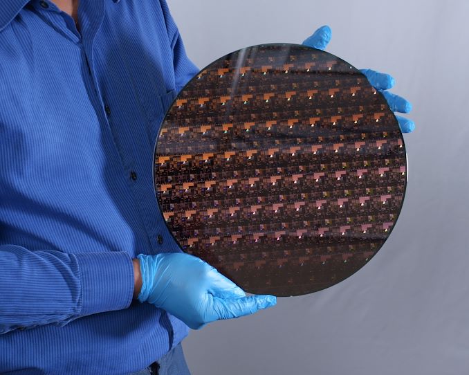
Every decade is the decade that tests the limits of Moore’s Law, and this decade is no different. With the arrival of Extreme Ultra Violet (EUV) technology, the intricacies of multipatterning techniques developed on previous technology nodes can now be applied with the finer resolution that EUV provides. That, along with other more technical improvements, can lead to a decrease in transistor size, enabling the future of semiconductors. To that end, Today IBM is announcing it has created the world’s first 2 nanometer node chip.
Names for Nodes
Just to clarify here, while the process node is being called ‘2 nanometer’, nothing about transistor dimensions resembles a traditional expectation of what 2nm might be. In the past, the dimension used to be an equivalent metric for 2D feature size on the chip, such as 90nm, 65nm, and 40nm. However with the advent of 3D transistor design with FinFETs and others, the process node name is now an interpretation of an ‘equivalent 2D transistor’ design.
Some of the features on this chip are likely to be low single digits in actual nanometers, such as transistor fin leakage protection layers, but it’s important to note the disconnect in how process nodes are currently named. Often the argument pivots to transistor density as a more accurate metric, and this is something that IBM is sharing with us.
Transistor Density
Today’s announcement states that IBM’s 2nm development will improve performance by 45% at the same power, or 75% energy at the same performance, compared to modern 7nm processors. IBM is keen to point out that it was the first research institution to demonstrate 7nm in 2015 and 5nm in 2017, the latter of which upgraded from FinFETs to nanosheet technologies that allow for a greater customization of the voltage characteristics of individual transistors.
IBM states that the technology can fit ’50 billion transistors onto a chip the size of a fingernail’. We reached out to IBM to ask for clarification on what the size of a fingernail was, given that internally we were coming up with numbers from 50 square millimeters to 250 square millimeters. IBM’s press relations stated that a fingernail in this context is 150 square millimeters. That puts IBM’s transistor density at 333 million transistors per square millimeter (MTr/mm2).
For comparison:
| Peak Quoted Transistor Densities (MTr/mm2) | ||||
| AnandTech | IBM | TSMC | Intel | Samsung |
| 22nm | 16.50 | |||
| 16nm/14nm | 28.88 | 44.67 | 33.32 | |
| 10nm | 52.51 | 100.76 | 51.82 | |
| 7nm | 91.20 | 237.18* | 95.08 | |
| 5nm | 171.30 | |||
| 3nm | 292.21* | |||
| 2nm | 333.33 | |||
| Data from Wikichip, Different Fabs may have different counting methodologies * Estimated Logic Density |
||||
As you can tell, different foundries have different official names with a variety of densities. It’s worth noting that these density numbers are often listed as peak densities, for transistor libraries where die area is the peak concern, rather than frequency scaling – often the fastest parts of a processor are half as dense as these numbers due to power and thermal concerns.
Stacked GAA
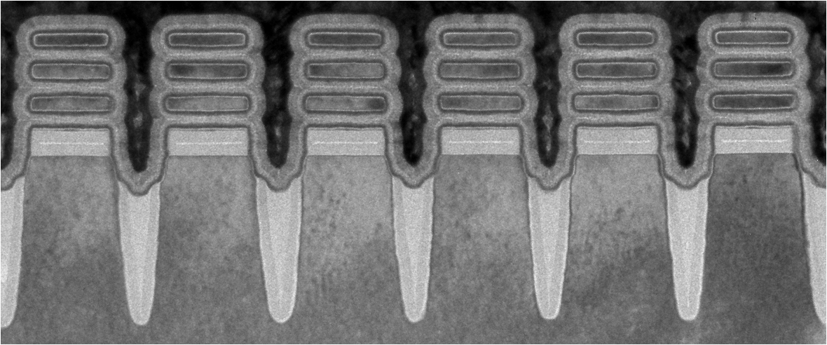
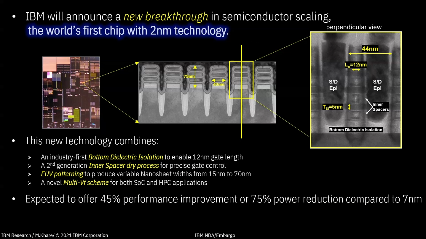
With regards the movement to Gate-All-Around / nanosheet transistors, while not explicitly stated by IBM, images show that this new 2nm processor is using a three-stack GAA design. Samsung is introducing GAA at 3nm, while TSMC is waiting until 2nm. Intel by contrast, we believe, will introduce some form of GAA on its 5nm process.
IBM’s 3-stack GAA uses a cell height of 75 nm, a cell width of 40 nm, and the individual nanosheets are 5nm in height, separated from each other by 5 nm. The gate poly pitch is 44nm, and the gate length is 12 nm. IBM says that its design is the first to use bottom dieletric isolation channels, which enables the 12 nm gate length, and that its inner spacers are a second generation dry process design that help enable nanosheet development. This is complimented by the first use of EUV patterning on the FEOL parts of the process, enabling EUV at all stages of the design for critical layers.
Users might be wondering why we’re hearing that IBM is the first to a 2nm chip. IBM is one of the world’s leading research centers on future semiconductor technology, and despite not having a foundry offering of their own, IBM develops IP in collaboration with others for their manufacturing facilities. IBM sold its manufacturing to GlobalFoundries with a 10 year partnership commitment back in 2014, and IBM also currently works with Samsung, and recently announced a partnership with Intel. No doubt the latter two will be partnering with IBM on some level around this new development for its viability in their own production chain.
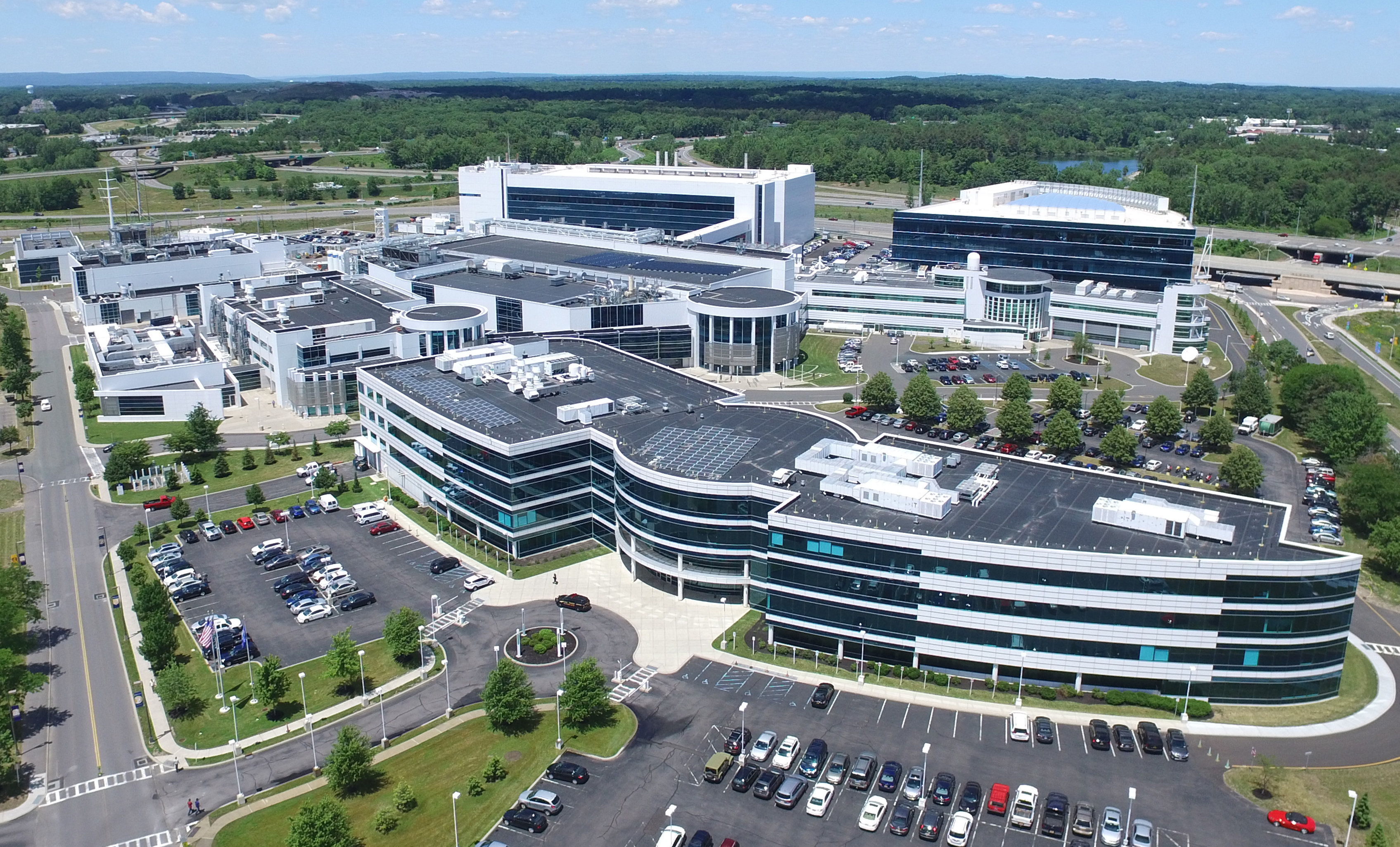
IBM Albany Research Center
No details on the 2nm test chip have been provided, although at this stage it is likely to be a simplified SRAM test vehicle with a little logic. The 12-inch wafer images showcase a variety of different light diffractions, which likely points to a variety of test cases to affirm the viability of the technology. IBM says that the test design uses a multi-Vt scheme for high-performance and high-efficiency application demonstrations.
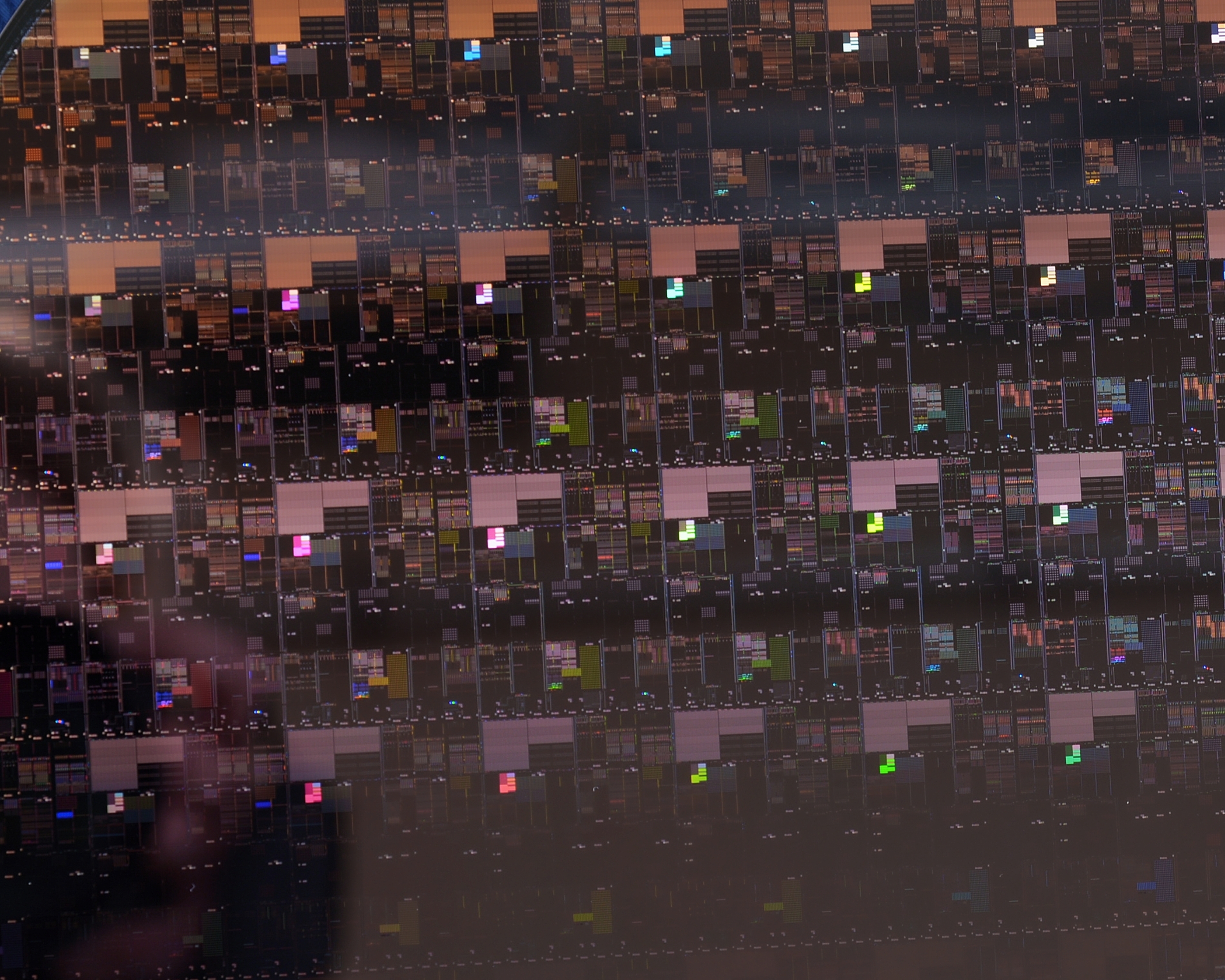
Wafer up close
The chip was designed and made at IBM’s Albany research facility, which features a 100,000 sq. ft. clean room. The purpose of this facility is to build on IBM’s expansive patent and licensing portfolio for collaborations with partners.
We have a set of questions with IBM’s experts awaiting response. We also now have an active invitation to go visit, as and when we can travel again.
Related Reading
- IBM and AMD to Advance Confidential Computing
- Hot Chips 2020 Live Blog: IBM z15, a 5.2 GHz Mainframe CPU (11:00am PT)
- IBM & Partners to Fight COVID-19 with Supercomputers, Forms COVID-19 HPC Consortium
- Hot Chips 31 Live Blogs: IBM's Next Generation POWER
- IBM to use Samsung 7nm EUV for Next-Gen POWER and z CPUs
- IBM And Everspin Announce 19TB NVMe SSD With MRAM Write Cache
- TSMC Update: 2nm in Development, 3nm and 4nm on Track for 2022
- Intel’s Manufacturing Roadmap from 2019 to 2029: Back Porting, 7nm, 5nm, 3nm, 2nm, and 1.4 nm


118 Comments
View All Comments
Matthias B V - Thursday, May 6, 2021 - link
Really curious to see GAA in real appliction chips and if it is as massive of an improvement as it looks.Probably not for density but performance and power consumption.
Also I am not sure if I got it right from Samsung but does it scale / perfroms especially better for SRAM than FinFET does? That would be a massive advantage!
Hifihedgehog - Thursday, May 6, 2021 - link
Exactly this. Display power generally dominates total system power consumption. Whoever wrote up that bio is trying too hard to create. Plus, IBM's stock has been receding since around 2012. So whenever they make some big promise about such and such, I take it with a boulder of salt. Making a one-off prototype is one thing. That happens sometimes as early as a decade in advance to real-world production! Actually delivering it consistently and competitively is a whole other matter entirely. The other big thing that has the alarm bells going off in my head for me right now is that their transistor density for 2nm is suspiciously close to TSMC's 3nm. I would not be surprised if Intel, through IBM, is trying to one up TSMC in perceived competitive edge who has used differing specifications to quote node size. And I would not be surprised if they are trying to reclaim their node leadership by stretching the truth a bit. Besides, TSMC's 3nm is already entering into production in 2022. When is IBM/Intel's 2nm even coming? If it's 2027, they might as well throw in the towel because TSMC will have already beat them to market with their comparable 3nm process by a good half a decade.Arsenica - Friday, May 7, 2021 - link
IBM has continued semiconductor R&R not with an aim in commercialization but rather to license the technology to others (via direct technology transfer or via patents).The patents product of this effort affect TSMC as much as anybody else so IBM doesn't care much about who beats who to market as they get their licensing fees anyway.
Hifihedgehog - Friday, May 7, 2021 - link
Already understood, but thanks for the explanation. I still suspect that Intel is somehow going to purchase rights to this, only to still be found trailing in manufacturing prowess by 3-5 years.Abe Dillon - Saturday, May 15, 2021 - link
Intel might not be as far behind as they seem. They've always been more stringent with their node specs than most of the rest of the industry. Its hard to compare one fab's node to another because there are so many variables, but at least in terms of density; you can see Intel's 10nm node is actually slightly better than TSMC's 7nm node.Maybe their transition to 7nm will go more smoothly than their transition to 10nm. Sometimes fab's just stumble on a transition.
From what I've heard, Intel's problems may be more insidious. I've heard the company culture is pretty toxic which demotivates everyone and can't be turned around so easily.
Anyway, supposedly Intel plans to start offering it's fab services to more third parties which means they have to market their tech better, so they'll probably loosen their stringent specifications for what qualifies as say, a 7nm or 5nm node. In the future I expect an Intel 5nm node to more closely resemble a TSMC 5nm node instead of a TSMC 3nm node for instance.
Santoval - Sunday, October 24, 2021 - link
"but at least in terms of density; you can see Intel's 10nm node is actually slightly better than TSMC's 7nm node."Not quite. Intel's 10nm process node has a slightly higher peak density than TSMC's first-gen (non-EUV) 7nm process node, but TSMC's 2nd gen 7nm+ node (with 6 EUV layers) has a markedly higher density of 114 MTr/mm2.
The table of the article is from Wikichip and does not report the peak densities of TSMC's 7nm+ node and Samsung's 5nm node. The following article from SemiWiki does though; SemiWiki also claims a slightly higher peak density of TSMC's 1st gen 7nm node at 96.5 Mtr/mm2 and TSMC's 5nm node at 173.1 Mtr/mm2 :
https://semiwiki.com/semiconductor-manufacturers/s...
rahvin - Sunday, May 9, 2021 - link
GAA is used extensively in radio chips (some of the chips in your average cell station are GAA) . GAA is capable of much higher frequencies than silicon. But it costs significantly more and it's toxic to handle and lithograph. The end result is it costs multiples more than silicon and is only used where it's higher frequencies make up for the cost impacts.shiva_c - Wednesday, May 12, 2021 - link
I think you are referring to a Galium based compound semiconductor while in the article GAA stands for Gate All Around.Matthias B V - Thursday, May 6, 2021 - link
Since IBM used to work with GF / SAMSUNG in the past and now also seems to collaborate more with Intel it would be interesting if / how this turns out for them taking on TSMC and if especially SAMSUNGs bet on GAA pays out...For me it looks like they didn't want to play catch up and just focused on 3nm GAA and less on 5nmLPE which is more of a 7nmLPU+. However if the numbers are right and the reduction of 50% for 3GAAE vs 7LPP is correct it would only be between TSMC 5 nm and TSMC3 nm but closer to their 5nm and similar to intels 7nm if you compare MTr/mm2 but maybe other factors are much better. Or they just take it safe and go more agressive with GAAP.
Also curious if Intel can manage their 5nm GAA by 2024/25 and therefore catch up with TSMC GAA...
Someone got insights on those?
rahvin - Sunday, May 9, 2021 - link
IBM's been neutral in semiconductor development, working with anyone that's willing to pay them for more than 20 years. They've been focused on the back end research for decades, their only fabs were mostly for specialized DOD chips or other products where the buyer could afford 10X the market rate for security of the chip design remaining in the US.