AMD 3rd Gen EPYC Milan Review: A Peak vs Per Core Performance Balance
by Dr. Ian Cutress & Andrei Frumusanu on March 15, 2021 11:00 AM ESTSection by Ian Cutress
CPU List and SoC Updates
In the past AMD has promoted its EPYC positioning in terms of single socket and dual socket setups, mostly on the basis that one of its larger processors can enable the same compute as two of Intel’s top-tier offerings. This time around, AMD actually does little direct comparison with Intel as to where its processors stand, instead focusing on the market optimizations for different elements of the market.
AMD market optimizations come in three main flavors: Core Performance, Core Density, Balanced and Optimized.
Every processor in AMD’s lineup will come with the following:
- 8 Channels of DDR4-3200
- 4 TB Memory Support (8 channel, 2DPC)
- 128 lanes of PCIe 4.0
- Simultaneous MultiThreading
- Performance Modes (Fixed Power) and Deterministic Modes (Fixed Frequency)
- 18G Infinity Fabric
- Secure Encrypted Virtualization with Secure Nested Pages
- Syncronized 1:1 Fabric and Memory Clock Speeds
Core Performance Optimized: 7xF3 Series
The Core Optimized processors were segmented out on the last page as a highlighted part of the processor lineup, now known as AMD’s F series of processors. These parts have F in the name, offer up to 32 cores, and the main focus here is on individual core performance peaks as well as sustained performance. Compared to other parts of a similar core count, these have higher TDP values, and charge a premium.
| AMD EPYC 7003 Processors Core Performance Optimized |
||||||
| Cores Threads |
Base Freq |
Turbo Freq |
L3 (MB) |
TDP | Price | |
| F-Series | ||||||
| EPYC 75F3 | 32 / 64 | 2950 | 4000 | 256 MB |
280 W | $4860 |
| EPYC 74F3 | 24 / 48 | 3200 | 4000 | 240 W | $2900 | |
| EPYC 73F3 | 16 / 32 | 3500 | 4000 | 240 W | $3521 | |
| EPYC 72F3 | 8 / 16 | 3700 | 4100 | 180 W | $2468 | |
For this review, one of the processors we have tested is the EPYC 75F3, the 32-core processor offering 4.0 GHz turbo, 2.95 GHz base frequency, and all 256 MB of L3 cache. This processor has four cores per chiplet active, and no doubt these processors use the best voltage/frequency response cores inside each chiplet as manufactured. The $4860 price point is above the $3761 for the next best 32-core processor, showcasing some of that premium.
Users will notice that the 16-core processor is more expensive ($3521) than the 24 core processor ($2900) here. This was the same in the previous generation, however in that case the 16-core had the higher TDP. For this launch, both the 16-core F and 24-core F have the same TDP, so the only reason I can think of for AMD to have a higher price on the 16-core processor is that it only has 2 cores per chiplet active, rather than three? Perhaps it is easier to bin a processor with an even number of cores active.
At the bottom is AMD’s sole 8-core offering, meaning only 1 core per chiplet, and zero contention for L3 cache. It also has a small range in frequency, which should enable deterministic workloads – despite the 180 W listed TDP, a 4.1 GHz Zen 3 core should not need more than 10 W per core, which leaves a lot of power for any configuration that wants to push the IO a little faster (more on that below).
All of these processors are aimed for systems that run software that is limited by single thread workloads, such as EDA tools, or for software that needs a lot of IO but can be limited by per-core licensing restrictions. All of these processors can be use in dual socket configurations.
Core Density Optimized: 48 Cores and Up
As part of the processor lineup, AMD is highlighting all of its high-core count products as being core density optimized, and systems built to take advantage of lower memory channel interleaving configurations (see below) could be built to the scale of 384 cores or 768 threads per 1U.
The new halo top-of-stack processor, the 64-core EPYC 7763, naturally fits into this segment. At 280 W, it adds another 40 W to the top processor publicly available from AMD, along with increasing both base frequency and turbo frequency as well as offering additional IPC gains. The price has increased by just under $1000 to represent where AMD believes it fits into this market.
| AMD EPYC 7003 Processors Core Density Optimized |
||||||
| Cores Threads |
Base Freq |
Turbo Freq |
L3 (MB) |
TDP | Price | |
| EPYC 7763 | 64 / 128 | 2450 | 3400 | 256 MB |
280 W | $7890 |
| EPYC 7713 | 64 / 128 | 2000 | 3675 | 225 W | $7060 | |
| EPYC 7663 | 56 / 112 | 2000 | 3500 | 240 W | $6366 | |
| EPYC 7643 | 48 / 96 | 2300 | 3600 | 225 W | $4995 | |
| P-Series (Single Socket Only) | ||||||
| EPYC 7713P | 64 / 128 | 2000 | 3675 | 256 | 225 W | $5010 |
AMD considers the EPYC 7763 as ‘a step up’ from the previous top-of-stack processor, the 7742. The direct replacement to the 64-core 7742 in this case is the 7713. We’ve tested both of the Milan and the 7742 Rome for this review, so we get to see how much of an uplift the new processors are.
Also part of the Core Density family is the first single socket processor, the 7713P. This is identical to the 7713, however does not support 2P configurations. As a result it comes in at $2000 cheaper.
The other interesting member of the family is the 7663, a 56 core processor. This configuration means that AMD is using 7 cores per chiplet, rather than the full 8, which is a configuration that AMD did not have with the previous generation. It would appear that AMD’s customers have requested a model like this, optimized for their workloads where less cache contention might be needed, or for workloads that won’t scale all the way to 64 cores.
Balanced and Optimized Portfolio
The rest of AMD’s portfolio of Milan processors comes under the ‘Balanced and Optimized’ banner, and this is where AMD will offer its 16-32 core processors as well as the rest of the 1P single socket parts.
| AMD EPYC 7003 Processors | ||||||
| Cores Threads |
Base Freq |
Turbo Freq |
L3 (MB) |
TDP | Price | |
| EPYC 7543 | 32 / 64 | 2800 | 3700 | 256 MB | 225 W | $3761 |
| EPYC 7513 | 32 / 64 | 2600 | 3650 | 128 MB | 200 W | $2840 |
| EPYC 7453 | 28 / 56 | 2750 | 3450 | 64 MB | 225 W | $1570 |
| EPYC 7443 | 24 / 48 | 2850 | 4000 | 128 MB |
200 W | $2010 |
| EPYC 7413 | 24 / 48 | 2650 | 3600 | 180 W | $1825 | |
| EPYC 7343 | 16 / 32 | 3200 | 3900 | 190 W | $1565 | |
| EPYC 7313 | 16 / 32 | 3000 | 3700 | 155 W | $1083 | |
| P-Series (Single Socket Only) | ||||||
| EPYC 7543P | 32 / 64 | 2800 | 3700 | 256 MB | 225 W | $2730 |
| EPYC 7443P | 24 / 48 | 2850 | 4000 | 128 MB | 200 W | $1337 |
| EPYC 7313P | 16 / 32 | 3000 | 3700 | 155 W | $913 | |
Almost all of these processors half the L3 cache to 128 MB, suggesting that these processors only have four active chiplets inside – this allows AMD to optimize its silicon product rather than providing lots of only-half enabled chiplets. This is seen perhaps in the price, as the 8-chiplet 32-core EPYC 7543 is almost $1000 more expensive than the EPYC 7513.
AMD only goes down to 16 cores here – the only 8 core processor is the 72F3 mentioned earlier. Also perhaps striking is that AMD does not go below 155 W TDP, which as we will see later in the review, might be down to some of the IO.
Bonus points for anyone spending $1337 on a processor like the EPYC 7443P.
Full Stack
For those wanting to see all the processors in one table with all the configurable TDP options, here we are. Processors we are testing in this review are highlighted in bold.
| AMD EPYC 7003 Processors | ||||||
| Cores Threads |
Frequency (GHz) |
L3 (MB) |
TDP (Default) / cTDP min / max |
Price | ||
| Base | Max | |||||
| EPYC 7763 | 64 / 128 | 2.45 | 3.40 | 256 ( 8 x 32 ) |
280 / 225 / 280 | $7890 |
| EPYC 7713 | 64 / 128 | 2.00 | 3.675 | 225 / 225 / 240 | $7060 | |
| EPYC 7663 | 56 / 112 | 2.00 | 3.50 | 240 / 225 / 240 | $6366 | |
| EPYC 7643 | 48 / 96 | 2.30 | 3.60 | 225 / 225 / 240 | $4995 | |
| EPYC 7543 | 32 / 64 | 2.80 | 3.70 | 225 / 225 / 240 | $3761 | |
| EPYC 7513 | 32 / 64 | 2.60 | 3.65 | 128 ( 4 x 32 ) |
200 / 165 / 200 | $2840 |
| EPYC 7453 | 28 / 56 | 2.75 | 3.45 | 64 ( 4 x 16 ) |
225 / 225 / 240 | $1570 |
| EPYC 7443 | 24 / 48 | 2.85 | 4.00 | 128 ( 4 x 32 ) |
200 / 165 / 200 | $2010 |
| EPYC 7413 | 24 / 48 | 2.65 | 3.60 | 180 / 165 / 200 | $1825 | |
| EPYC 7343 | 16 / 32 | 3.20 | 3.90 | 190 / 165 / 200 | $1565 | |
| EPYC 7313 | 16 / 32 | 3.00 | 3.70 | 155 / 155 / 180 | $1083 | |
| F-Series | ||||||
| EPYC 75F3 | 32 / 64 | 2.95 | 4.00 | 256 ( 8 x 32 ) |
280 / 225 / 280 | $4860 |
| EPYC 74F3 | 24 / 48 | 3.20 | 4.00 | 240 / 225 / 240 | $2900 | |
| EPYC 73F3 | 16 / 32 | 3.50 | 4.00 | 240 / 225 / 240 | $3521 | |
| EPYC 72F3 | 8 / 16 | 3.70 | 4.10 | 180 / 165 / 200 | $2468 | |
| P-Series (Single Socket Only) | ||||||
| EPYC 7713P | 64 / 128 | 2.00 | 3.675 | 256 ( 8 x 32 ) |
225 / 225 / 240 | $5010 |
| EPYC 7543P | 32 / 64 | 2.80 | 3.70 | 225 / 225 / 240 | $2730 | |
| EPYC 7443P | 24 / 48 | 2.85 | 4.00 | 128 ( 4 x 32 ) |
200 / 165 / 200 | $1337 |
| EPYC 7313P | 16 / 32 | 3.00 | 3.70 | 155 / 155 / 180 | $913 | |
To fill in some of the demands in costs and offering, AMD is also planning to supply 2nd Gen EPYC into the market for a good time, enabling both platforms for customers. These include the 32-core 7532, 24-core 7352, 16-core 7282, and a couple of 8-core processors.
Comparing Gen-on-Gen Pricing
Direct comparisons are always made against the previous generation, and these are the suggested comparisons:
| AMD Third Gen EPYC ("Milan") |
AMD Second Gen EPYC ("Rome") |
|||||||||
| Cores | Freq | TDP (W) |
Price | AMD | Cores | Freq | TDP | Price | ||
| Milan | Rome | |||||||||
| 7763 | 64 | 2.45/3.50 | 280 | $7890 | 7H12 | 64 | 2.60/3.30 | 280 | - | |
| 7742 | 64 | 2.25/3.40 | 225 | $6950 | ||||||
| 7713 | 64 | 2.0/3.675 | 225 | $7060 | 7702 | 64 | 2.00/3.35 | 200 | $6450 | |
| 7662 | 64 | 2.00/3.30 | 225 | $6150 | ||||||
| 7663 | 56 | 2.00/3.50 | 240 | $6366 | ||||||
| 7643 | 48 | 2.30/3.60 | 225 | $4995 | 7642 | 48 | 2.30/3.30 | 225 | $4775 | |
| 7552 | 48 | 2.20/3.30 | 200 | $4025 | ||||||
| 7543 | 32 | 2.80/3.70 | 225 | $3761 | 7542 | 32 | 2.90/3.40 | 225 | $3400 | |
| 7532 | 32 | 2.40/3.30 | 200 | $3350 | ||||||
| 7513 | 32 | 2.60/3.65 | 200 | $2840 | 7502 | 32 | 2.50/3.35 | 180 | $2600 | |
| 7452 | 32 | 2.35/3.35 | 155 | $2025 | ||||||
| 7453 | 28 | 2.75/3.45 | 225 | $1570 | ||||||
| 7443 | 24 | 2.85/4.00 | 200 | $2010 | 7402 | 24 | 2.80/3.35 | 180 | $1783 | |
| 7413 | 24 | 2.65/3.60 | 180 | $1825 | ||||||
| 7352 | 24 | 2.30/3.20 | 155 | $1350 | ||||||
| 7343 | 16 | 3.20/3.90 | 190 | $1565 | ||||||
| 7313 | 16 | 3.00/3.70 | 155 | $1083 | ||||||
| 7302 | 16 | 3.00/3.30 | 155 | $978 | ||||||
| 7282 | 16 | 2.80/3.20 | 120 | $650 | ||||||
Overall there is an uptick from Rome to Milan on pricing.
New Features and SoC Design
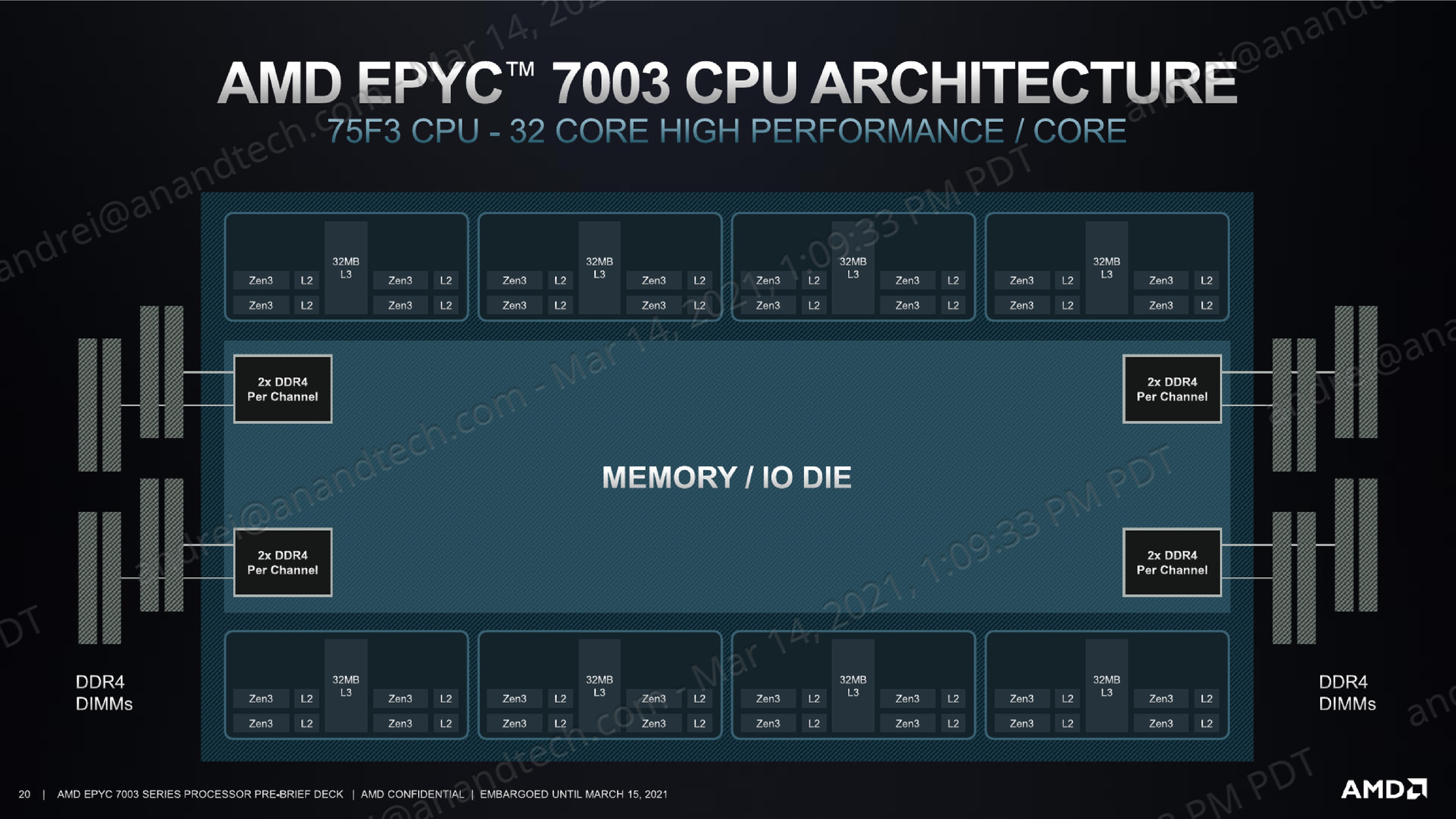
In our interview with AMD’s Forrest Norrod, he explained that the original goal of Milan was to update Rome’s 8-core chiplets from Zen 2 to Zen 3, but a number of factors meant that the central IO die also received updates, both on the power side and for Infinity Fabric performance.
Beyond the core updates from Zen 2 to Zen 3, which we’ve covered extensively in our consumer coverage, AMD has enabled several key features with Milan.
Memory Interleaving for 4/6/8 Channel Configurations
The enterprise and datacenter markets involve a vast array of potential workloads, some are compute-bound, some are memory-bound, but the goal has always been to get the work done as quickly as possible, as efficiently as possible, and as cheaply as possible. The larger companies will often optimize their deployments in every way imaginable, and that includes memory.
AMD admits that there is a portion of the market that is very much memory-bound, either in capacity, latency, or bandwidth. These customers will keep demanding higher capacity support, faster memory, or just more memory channels for both capacity or bandwidth. We’ve been told that there is a holistic split at some level between these sorts of customers, and those that are simply compute-bound, which may come to a head with differentiated products in the future. But for now, we have eight-channel DDR4 processors on the market, which is not-enough for some customers, but plenty for others who don’t need all that capacity or bandwidth.
It’s the latter customers where optimizations may occur. For example, if memory bandwidth or capacity is not a limiting factor, then those customers can design systems with fewer memory channels being used. This helps by increasing density, making physical system design simpler, perhaps cooling, but also by disabling those memory channels, more power is available for their compute-bound systems. We came to a point in the previous generation lifecycle where we were starting to see motherboards enter the market with fewer than eight memory slots for these reasons.
In order to get the best performance, or reliable performance, from the memory (and not experience any NUMA or silo effects), the memory installed needs to have effective memory interleaving enabled on what is installed. AMD EPYC in the past has supported 8-channel interleaving and 4-channel interleaving, but for Milan, AMD is also supporting 6-channel interleaving for customers that build in those configurations. Four and Eight are obvious powers of two for AMD to have included by default, but enough demand for Six was there to enable an update to the IO die to support this mode.
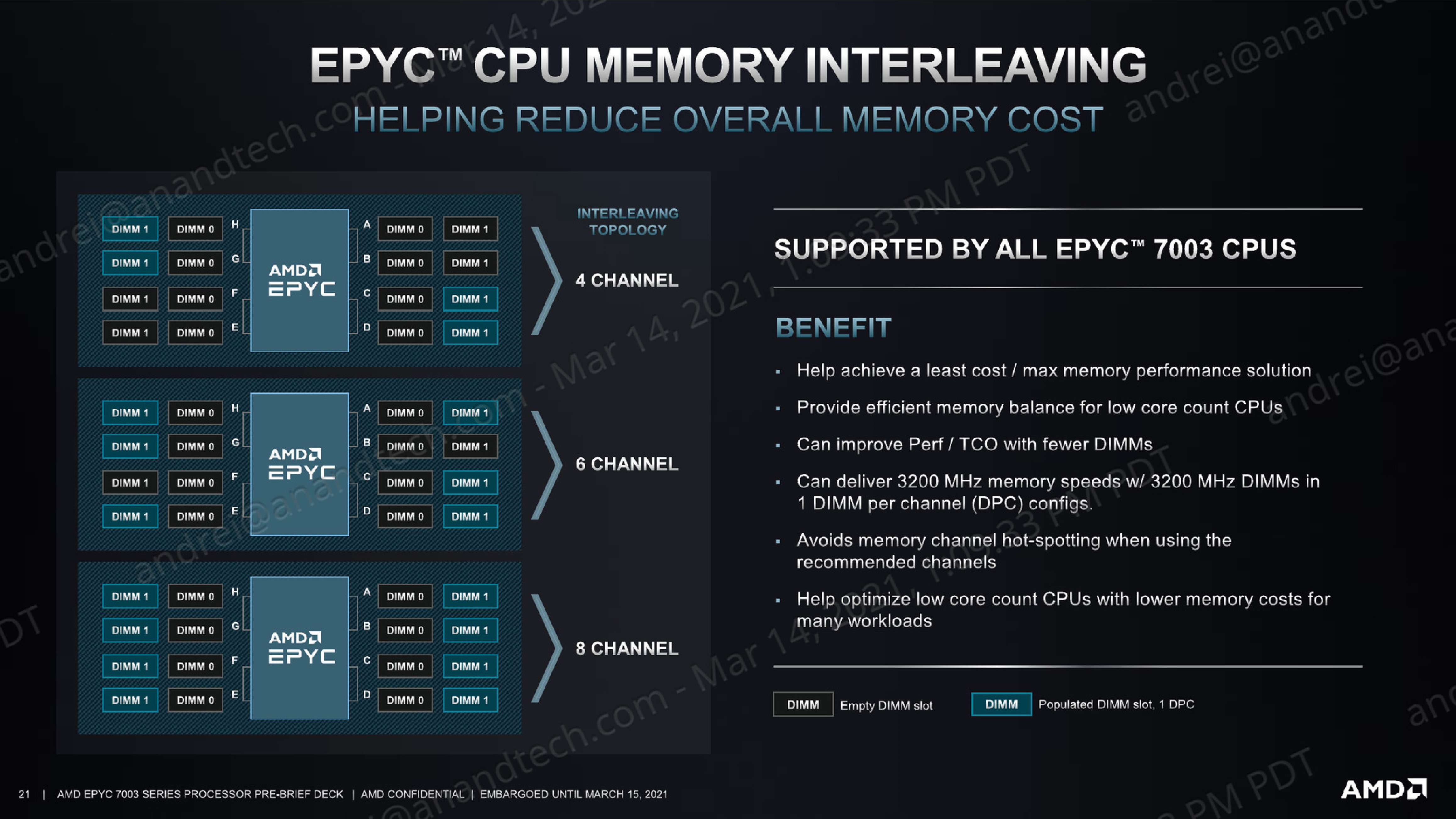
AMD has confirmed that 6-channel memory interleaving, when using one module per channel, will be supported on all Milan processors.
Security for Return Programming and Secure Nested Pages
The effects of Spectre, Meltdown, and its variants have repurposed processor security to be more proactive at all the major microprocessor designers and manufacturers. AMD has implemented fixes in hardware for the Spectre variants to which it was susceptible, and hasn’t needed to add additional protection from Meltdown and its variants as AMD CPUs are not naturally vulnerable.
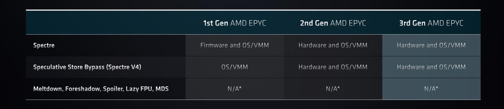
The new segment of attacks beyond these are based on return address programming, and effectively adjusting the control flow of code on the processors by manipulating stack return addresses or jump/control commands. AMD implemented a fix for these sorts of attacks in its Zen 3 core, and these fixes get passed into EPYC Milan, known as ‘Shadow Stacks’. These are hardware based solutions, enabling a minimal effect to performance, but absolutely required for security.
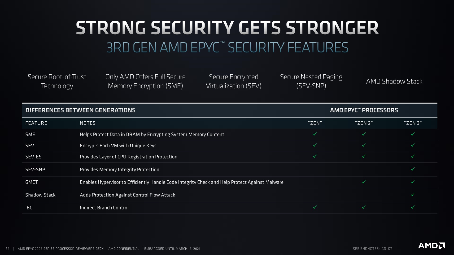
The other segment to AMD’s security updates is Secure Nested Paging, part of AMD’s Secure Encrypted Virtualization technology. These technologies all deal with hyperscalers enabling multiple host instances on a single system, and being able to protect the instances from each other. In previous generation Rome, Secure Encrypted Virtualization allowed a secure hypervisor to isolate these instances or virtual machines from each other in a secure and encrypted way (hence the name).
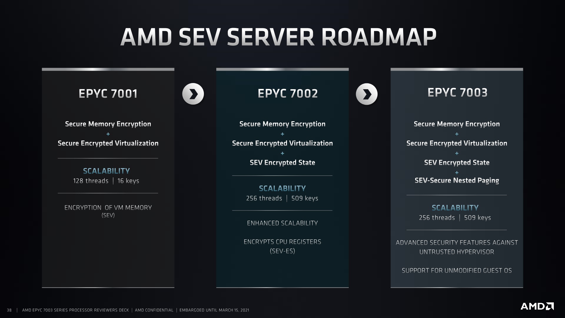
Secure Nested Paging takes this one stage further, and enables additional security of the virtual machines from the hypervisor itself. This allows protection against an untrusted hypervisor, should an attacker get access, as well as support for software running on unmodified guest operating systems for which the software was originally not built for.
Enhanced Memory and IO Performance
One of the big updates from the Zen 2 core complex to the Zen 3 core complex in all of AMD’s product families was the size of that complex, moving from four cores to eight cores. This means that in an eight core chiplet, rather than there being two complexes of four cores and a separated L3 cache, there is now a single eight core complex with a unified cache. As seen in our consumer reviews, this matters a lot for memory-heavy operation as well as branch heavy code. Another benefit is that the control electronics for the complex are now at the edge of the chiplet, providing some small improvement.
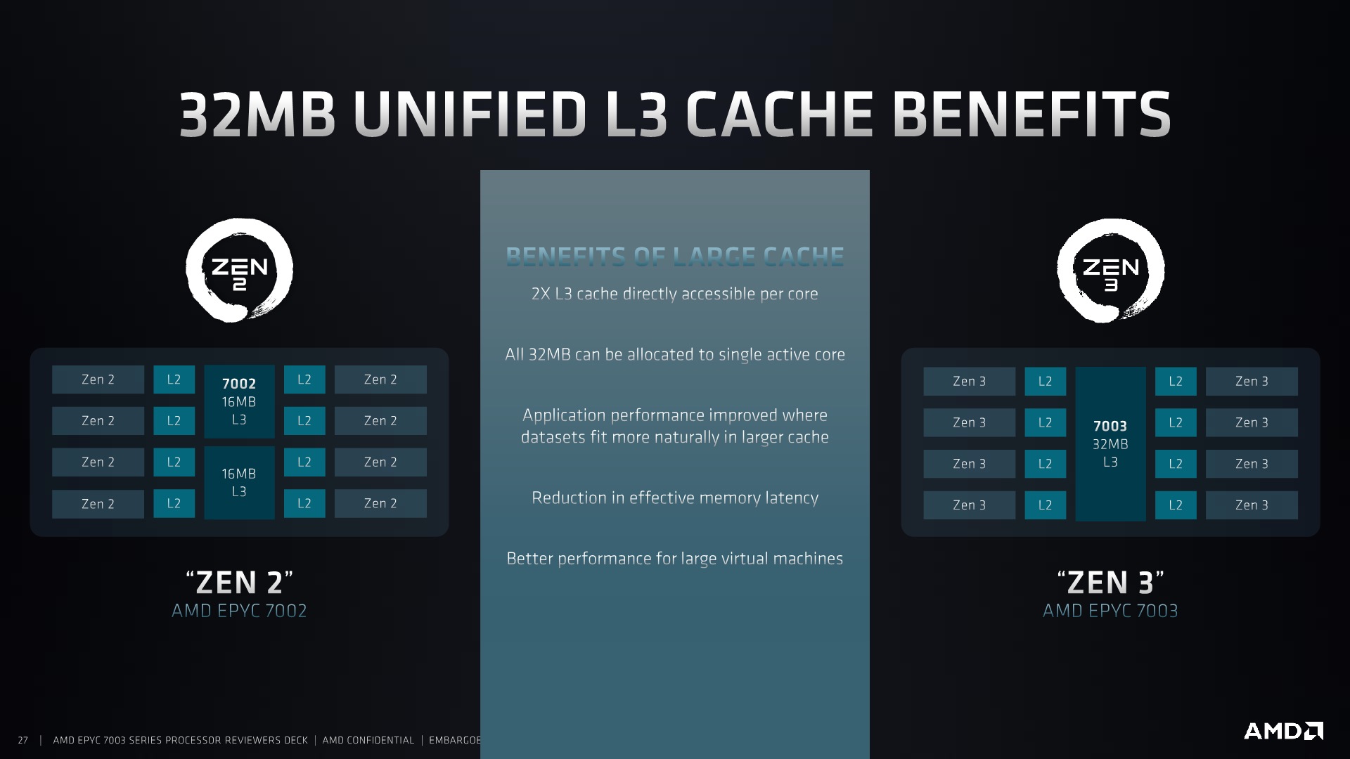
We’ll go into how exactly the cache structure changes later in the review.
The other angle to Milan’s performance in IO is on the Infinity Fabric and PCIe. For this generation, AMD has enabled 18 Gbps Infinity Fabric links over its SERDES connections, up from the previous generation 16 Gbps links. This might come across as slightly minor, but it should enable better performance in a competitive core-to-core communications environment.
AMD is also supporting Extended Speed Modes on its PCIe links with Milan. This is part of the PCIe 4.0 standard, and allows customers to enable more bandwidth over the PCIe link to discrete accelerator cards if the motherboard is designed to support those speeds. This requires extra power from the processor, which does take power/performance away from the processor cores, however AMD has stated that because its customers have so many different optimization points, a number of workloads will benefit from this option.
Other Improvements and ISA Enhancements
Also on AMD’s list of updates to Milan are the following:
| INVLPGB | New instruction to use instead of inter-core interrupts to broadcast page invalidates, requires OS/hypervisor support |
| VAES / VPCLMULQDQ | AVX2 Instructions for encryption/decryption acceleration |
| SEV-ES | Limits the interruptions a malicious hypervisor may inject into a VM/instance |
| Memory Protection Keys | Application control for access-disable and write-disable settings without TLB management |
| Process Context ID (PCID) | Process tags in TLB to reduce flush requirements |
| INT8 | Dual INT8 pipes, up from 1, doubles INT8 performance |


120 Comments
View All Comments
mkbosmans - Tuesday, March 23, 2021 - link
Even if you have a nice two-tiered approach implemented in your software, let's say MPI for the distributed memory parallelization on top of OpenMP for the shared memory parallelization, it often turns out to be faster to limit the shared memory threads to a single socket of NUMA domain. So in case of an 2P EPYC configured as NPS4 you would have 8 MPI ranks per compute node.But of course there's plenty of software that has parallelization implemented using MPI only, so you would need a separate process for each core. This is often because of legacy reasons, with software that was originally targetting only a couple of cores. But with the MPI 3.0 shared memory extension, this can even today be a valid approach to great performing hybrid (shared/distributed mem) code.
mode_13h - Tuesday, March 23, 2021 - link
Nice explanation. Thanks for following up!Andrei Frumusanu - Saturday, March 20, 2021 - link
This is vastly incorrect and misleading.The fact that I'm using a cache line spawned on a third main thread which does nothing with it is irrelevant to the real-world comparison because from the hardware perspective the CPU doesn't know which thread owns it - in the test the hardware just sees two cores using that cache line, the third main thread becomes completely irrelevant in the discussion.
The thing that is guaranteed with the main starter thread allocating the synchronisation cache line is that it remains static across the measurements. One doesn't actually have control where this cache line ends up within the coherent domain of the whole CPU, it's going to end up in a specific L3 cache slice depended on the CPU's address hash positioning. The method here simply maintains that positioning to be always the same.
There is no such thing as core-core latency because cores do not snoop each other directly, they go over the coherency domain which is the L3 or the interconnect. It's always core-to-cacheline-to-core, as anything else doesn't even exist from the hardware perspective.
mkbosmans - Saturday, March 20, 2021 - link
The original thread may have nothing to do with it, but the NUMA domain where the cache line was originally allocated certainly does. How would you otherwise explain the difference between the first quadrant for socket 1 to socket 1 communication and the fourth quadrant for socket 2 to socket 2 communication?Your explanation about address hashing to determine the L3 cache slice may be makes sense when talking about fixing the inital thread within a L3 domain, but not why you want that that L3 domain fixed to the first one in the system, regardless of the placement of the two threads doing the ping-ponging.
And about core-core latency, you are of course right, that is sloppy wording on my part. What I meant to convey is that roundtrip latency between core-cacheline-core and back is more relevant (at least for HPC applications) when the cacheline is local to one of the cores and not remote, possibly even on another socket than the two thread.
Andrei Frumusanu - Saturday, March 20, 2021 - link
I don't get your point - don't look at the intra-remote socket figures then if that doesn't interest you - these systems are still able to work in a single NUMA node across both sockets, so it's still pretty valid in terms of how things work.I'm not fixing it to a given L3 in the system (except for that socket), binding a thread doesn't tell the hardware to somehow stick that cacheline there forever, software has zero say in that. As you see in the results it's able to move around between the different L3's and CCXs. Intel moves (or mirrors it) it around between sockets and NUMA domains, so your premise there also isn't correct in that case, AMD currently can't because probably they don't have a way to decide most recent ownership between two remote CCXs.
People may want to just look at the local socket numbers if they prioritise that, the test method here merely just exposes further more complicated scenarios which I find interesting as they showcase fundamental cache coherency differences between the platforms.
mkbosmans - Tuesday, March 23, 2021 - link
For a quick overview of how cores are related to each other (with an allocation local to one of the cores), I like this way of visualizing it more:http://bosmans.ch/share/naples-core-latency.png
Here you can for example clearly see how the four dies of the two sockets are connected pairwise.
The plots from the article are interesting in that they show the vast difference between the cc protocols of AMD and Intel. And the numbers from the Naples plot I've linked can be mostly gotten from the more elaborate plots from the article, although it is not entirely clear to me how to exactly extend the data to form my style of plots. That's why I prefer to measure the data I'm interested in directly and plot that.
imaskar - Monday, March 29, 2021 - link
Looking at the shares sinking, this pricing was a miss...mode_13h - Tuesday, March 30, 2021 - link
Prices are a lot easier to lower than to raise. And as long as they can sell all their production allocation, the price won't have been too high.Zone98 - Friday, April 23, 2021 - link
Great work! However I'm not getting why in the c2c matrix cores 62 and 74 wouldn't have a ~90ns latency as in the NW socket. Could you clarify how the test works?node55 - Tuesday, April 27, 2021 - link
Why are the cpus not consistent?Why do you switch between 7713 and 7763 on Milan and 7662 and 7742 on Rome?
Why do you not have results for all the server CPUs? This confuses the comparison of e.g. 7662 vs 7713. (My current buying decision )