AMD Zen 3: An AnandTech Interview with CTO Mark Papermaster
by Dr. Ian Cutress on October 16, 2020 9:00 AM EST
The announcement of the new Ryzen 5000 processors, built on AMD’s Zen 3 microarchitecture, has caused waves of excitement and questions as to the performance. The launch of the high-performance desktop processors on November 5th will be an interesting day. In advance of those disclosures, we sat down with AMD’s CTO Mark Papermaster to discuss AMD’s positioning, performance, and outlook.
 Dr. Ian Cutress AnandTech |
 Mark Papermaster AMD |
We’ve interviewed Mark a number of times before here at AnandTech, such as at the launch of second generation EPYC or looking at AMD’s 2020 prospects (and a couple of discussions that were never published). Mark is always very clear on what the vision of AMD’s roadmaps are, as always likes to highlight some of the key areas of AMD’s expertise that sometimes don’t hit the standard column inches.
With the launch of Zen 3, and the Ryzen 5000 family, the key headline that AMD is promoting is an absolute desktop high-performance leadership, across workloads, gaming, and energy efficiency. It puts AMD in a position the company hasn’t held for at least 15 years, if the numbers are true. As part of the launch event, the AMD team reached out if we had some questions for Mark. Indeed we do.
You can read our launch day coverage here:
AMD Ryzen 5000 and Zen 3 on Nov 5th: +19% IPC, Claims Best Gaming CPU
IC: When I interviewed Lisa at the crest of that first generation Ryzen launch, she mentioned how AMD’s positioning helped the company to think outside the box to develop its new high-performance x86 designs. Now that AMD is claiming market performance leadership, how do AMD’s engineering teams stay grounded and continue to drive that out-of-the-box thinking?
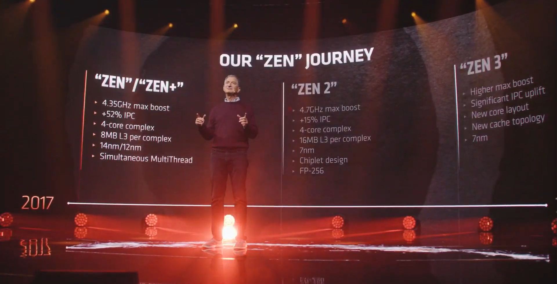
MP: Of our team we are very proud - they are one of the most innovative engineering teams in the industry. So this is a hard fought battle to get into this leadership position with Zen 3 and I can tell you we have a very strong roadmap going forward. The team indeed is staying very very grounded - you look at the kind of approach that we took on Zen 3, and you know it wasn’t any one silver bullet that delivered the performance [uplift], it was really touching almost every unit across the CPU and the team did an excellent job of driving improvements in performance, improvements in efficiency, reducing the latency to memory, and providing a tremendous improvement in performance.
[We achieved] a 19% in a single generation of instruction per clock over our previous generation, which was Zen 2 released just mid of last year. So it was a phenomenal achievement, and it’s that focus on what I’ll call ‘hardcore engineering’ that the team will continue going forward - it won’t be about silver bullets, it will be about continuing to provide real-world performance gains to our customers.
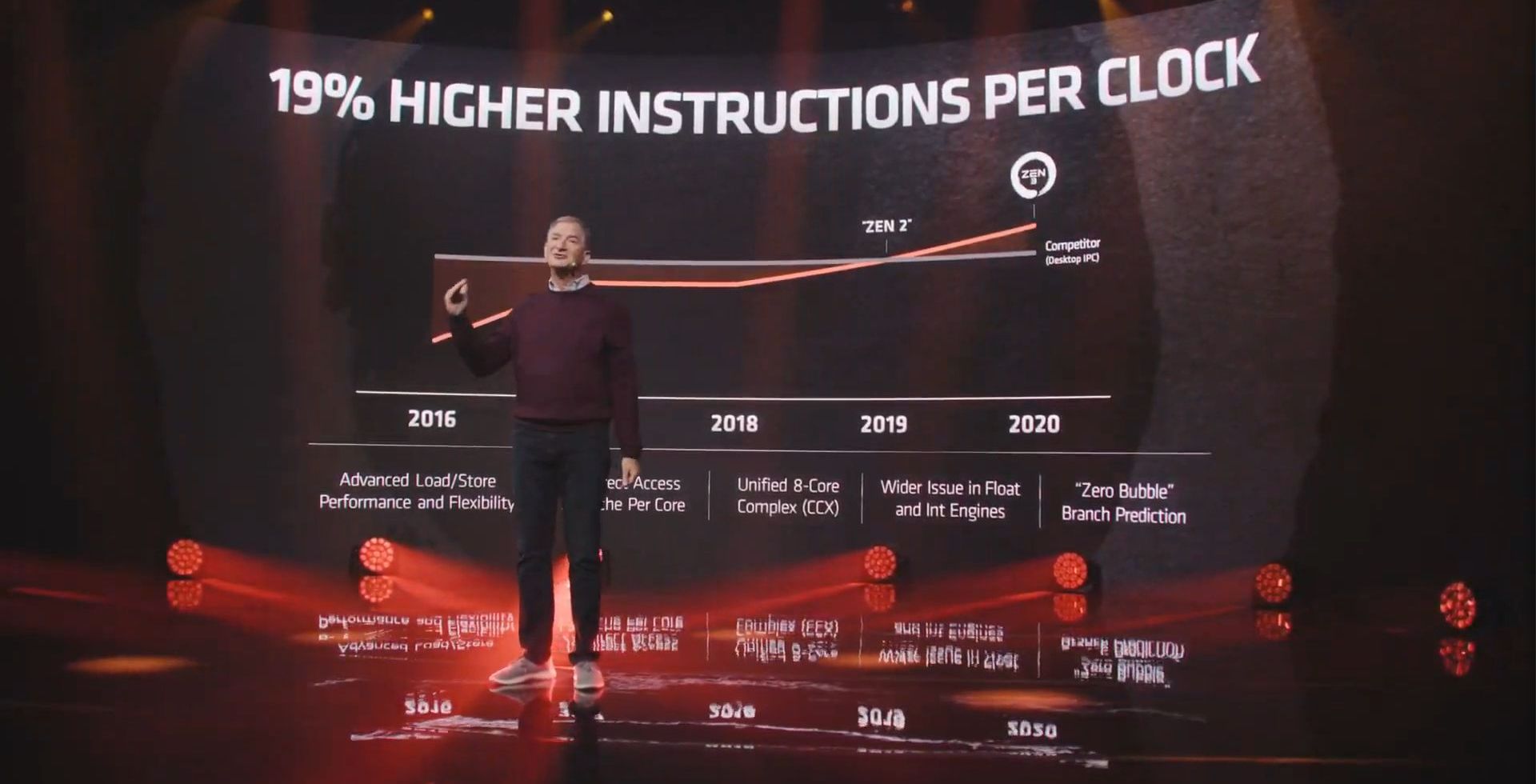
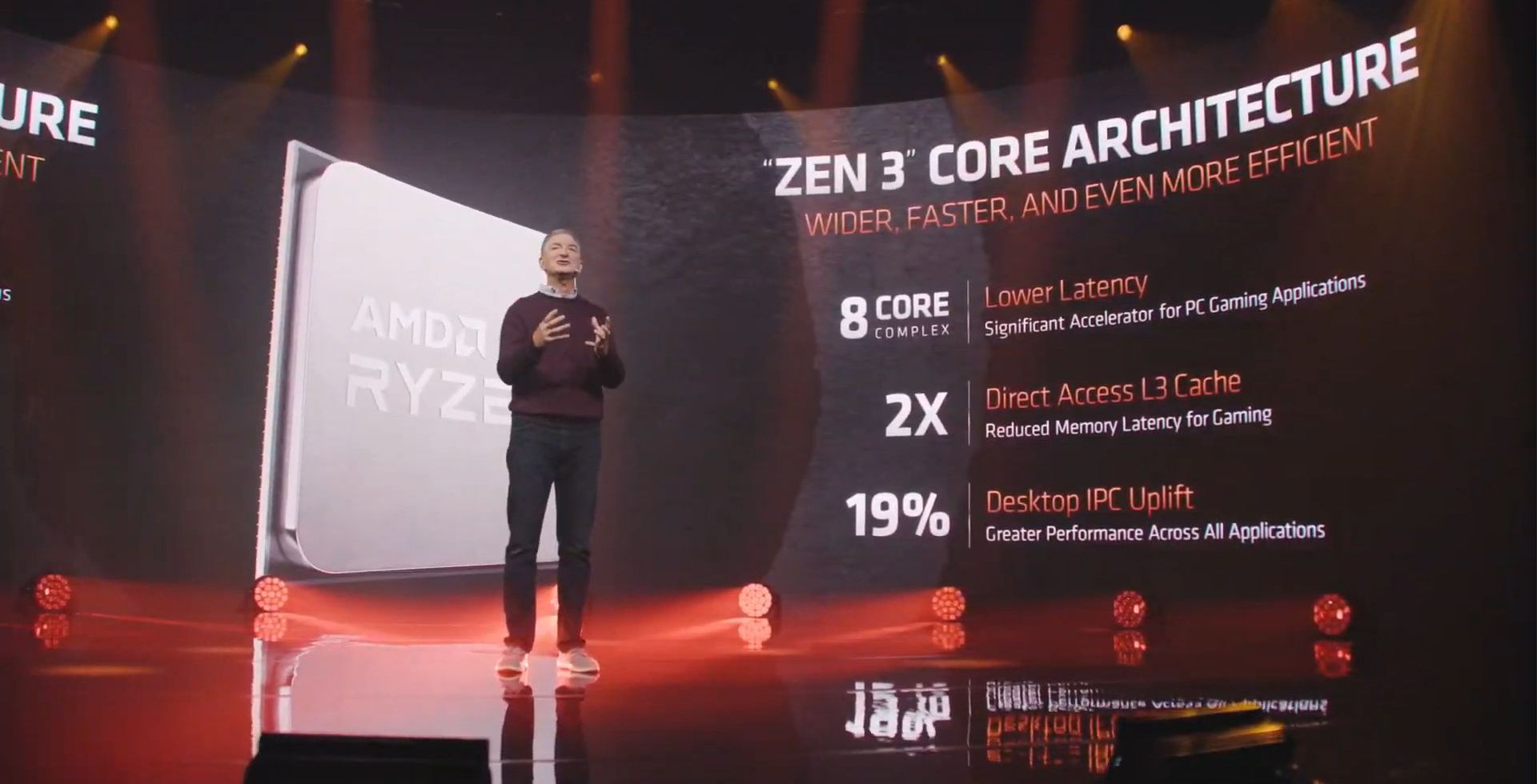
IC: To highlight that 19% value: two of those highlights of AMD’s announcements include the +19% increase in raw performance per clock compared to Zen 2, but also this new core complex design with eight cores and 32 MB of L3 cache. To what extent is the larger core complex helping with the raw performance increase, or are there other substantial benefits in the design by moving to the combined CCX?
MP: The change in the basic construct of the core complex was very very important in allowing us to realize reductions in latency to memory which is huge for gaming. Gaming is a huge market for us in high performance desktop and games typically have a dominant thread - and so that dominant thread, its performance is very dependent on the L3 cache available to it. This is because if it can hit in that local L3 cache, obviously it’s not traversing all the way out to main memory. So by reorganizing our core complex and doubling it to four cores that have direct access to 16 MB L3 cache, by now having eight cores that have direct access to a 32 MB of L3 cache you really - it’s the single biggest lever in reducing latency. Obviously when you hit in the cache you provide effective latency - it directly improves performance. It was a big lever for gaming, but we had a number of levers behind that - again we really touched every unit in the CPU.
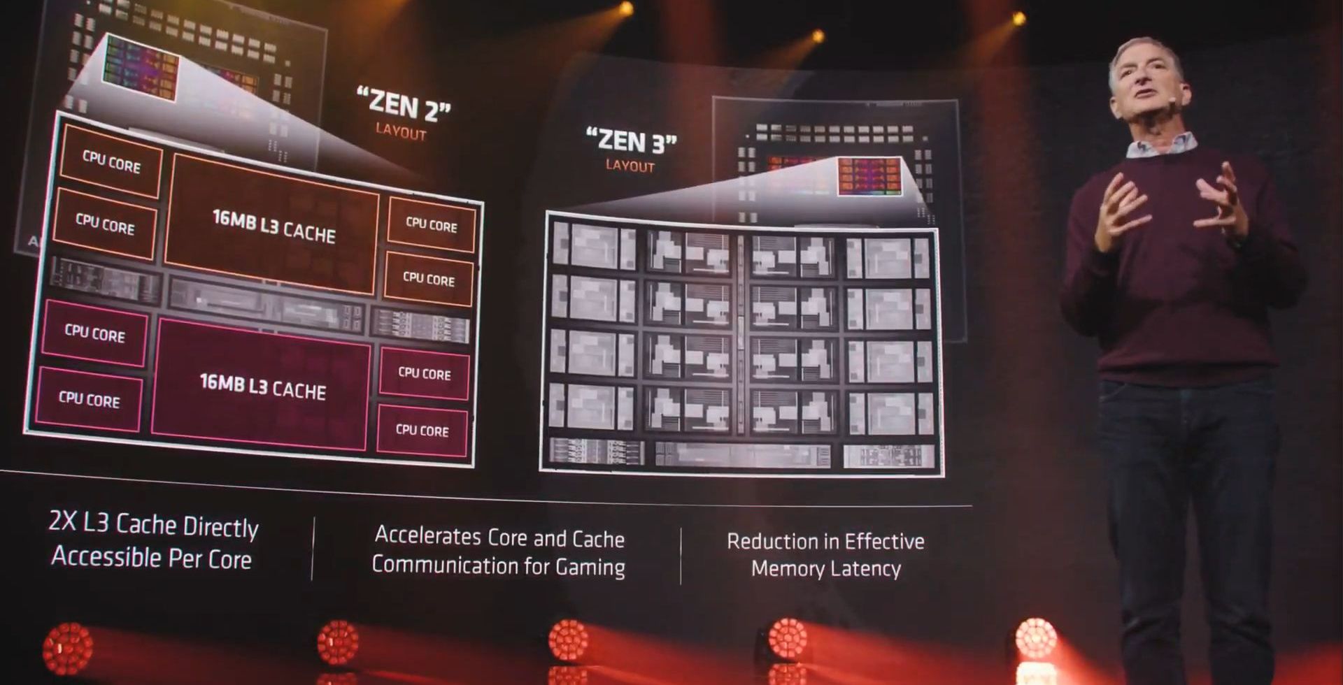
IC: Doubling that L3 cache access for each core, from 16 MB to 32 MB, is a sizable leap I’ll grant you that! It improves that overall latency up to 32 MB as you’ve said so we don’t have to go out to main memory. But has doubling the size affected the L3 latency range at all? Obviously there are tradeoffs when you double an L3 cache, even so when you have more cores accessing it.
MP: The team did an excellent job on engineering, both logically and physically. That’s always the key - how to architect the reorganization, so to change the logic to support this new structure and equally focus on the physical implementation - how do you optimize layout so you’re not adding stages of delay that would effectively neuter the gains? It was tremendous engineering on the reorganization on the Zen 3 core that truly delivers the benefit in reduced latency.
I’ll go beyond that - as we talk about physical implementation, the normal thinking would be when you add the amount of logic changes that we did to achieve that 19% IPC, normally of course the power envelope would go up. We didn’t change technology nodes - we stayed in 7nm. So I think your readers would have naturally assumed therefore we went up significantly in power but the team did a phenomenal job of managing not just the new core complex but across every aspect of implementation and kept Zen 3 in the power envelope that we had been in Zen 2.
When you look at Ryzen as it goes out, we are able to stay in the same AM4 socket and that same power envelope and yet deliver these very very significant performance gains.
IC: Speaking to that process node, TSMC’s 7nm as you said: we’ve specifically been told that it is this sort of minor process update that was used for Ryzen 3000XT. Are there any additional benefits that Ryzen 5000 is getting through the manufacturing process that perhaps we are not aware of?
MP: It is in fact the core is in the same 7nm node, meaning that the process design kit [the PDK] is the same. So if you look at the transistors, they have the same design guidelines from the fab. What happens of course in any semiconductor fabrication node is that they are able to make adjustments in the manufacturing process so that of course is what they’ve done, for yield improvements and such. For every quarter, the process variation is reduced over time. When you hear ‘minor variations’ of 7nm, that is what is being referred to.
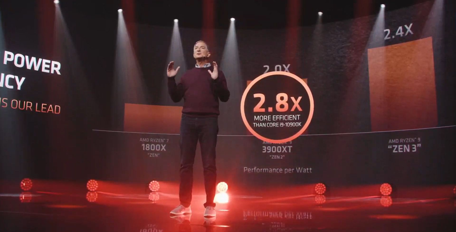
IC: Moving from Zen 2 to Zen 3, the headline number in the improvement of performance per watt is 24% on top of the 19% IPC. This obviously means that there have been additional enhancements made at the power deliver level - can you talk to any of those?
MP: We have a tremendous focus on our power management. We have an entire microcontroller and power management schema that we have across the entire CPU. We enhance that every generation, so we’re very proud of what the Zen 3 team has done to achieve this 24% power improvement. It is yet more advances in whole Precision Boost to give us more granularity in managing both frequency and voltage while constantly listening to the myriad of sensors that we have on the chip. It is yet more granularity and the adaptability of our power management to the workload that our users are running on the microprocessor. So it is more responsive, and being more responsive means that it also delivers more efficiency.
IC: One of the points made on Zen 2 was a relatively high idle power draw of the IO die, anywhere from 13 W to 20 W. We’ve been told that this time around Zen 3 uses the same IO die as Zen 2 did. We just wanted to confirm that does Zen 3 change anything in this regard, given the focus on power efficiency and performance per watt, or is it the same design for the sake of compatibility or cost effectiveness?
MP: These are incremental advancements on the IO die that allowed us to give our customers in high performance desktop, to leverage that AM4 socket while getting these performance gains - that was a very calculated move to deliver CPU performance while giving continuity to our customer base. We are constantly driving power efficiency - with Zen 3 the focus was on the core and the core-cache complex in driving the bulk of our power efficiency.
IC: Can you talk about AMD’s goals with regards to IO and power consumption - we’ve seen AMD deliver PCIe Gen4 in 7nm but the IO die is still based in 12/14nm from Global Foundries. I assume it is a key target for improvements in the future just not this time around?
MP: It’s generational - if you look to the future we drive improvements in every generation. So you will see AMD transition to PCIe Gen 5 and that whole ecosystem. You should expect to hear from us in our next round of generational improvements across both the next-gen core that is in design as well as that next-gen IO and memory controller complex.
IC: Speaking about the chiplet itself, the AMD presentation gave us a high-level view of the increased core complex. We’ve noted that the off-chip communication for those chiplets has now been moved from the center of between the two core complexes to the edge. Are there any specific benefits to this, such as wire latency, or power?
MP: You look at that optimization trade-off, marrying the logical implementation with the physical implementation. So the new cache core complex was designed to minimize latency from the CPU cores themselves into that cache complex. To put the control circuits being placed where they are means the longer wire lengths can go to the less latency sensitive circuits.
IC: Over the last couple of years, AMD has presented that it has a roadmap when it comes to its Infinity Fabric design, such as striving towards the two typical areas of higher bandwidth and better efficiency. Does Zen 3 and the new Ryzen 5000 family have any updates to the IF over Ryzen 3000?
MP: We do - we made improvements, you’ll see new security elements that will be rolling out. We boosted our security, [and] we are always tuning our Infinity Architecture. With Zen 3 the focus was on delivering the raw CPU performance. So in terms of our Infinity Architecture for Ryzen desktop it’s incremental, and we’ll be rolling out some of those details - we’ve very excited about it and it’s a great compliment to the main headline story, which is CPU performance leadership.
IC: With AMD and Intel, we’re now seeing both companies binning the silicon from the fabs to within an inch of its maximum - leaving very little overclocking headroom just so users have that peak performance straight out of the box. From your perspective how do features such as the Precision Boost Overdrive, where frequencies go above the stated range on the box - how do features like that evolve or do they just slowly disappear as binning optimization and knowledge increases over time?
MP: Of course our goal is to maximize what we support with our maximum boost frequency. With Zen 3 we do increase that to 4.9 GHz. We’re always focused on improving our binning - the way you should think about it is [that] we’ll always have the best boost frequency that we can provide, and it is tested across the full gamut of workloads. Our test suite tries to cover literally every type of workload that we believe our customers would be able to run on our CPU. But end-users are very smart, and they might have a segment of those applications, and our thought is that we will continue to provide overclocking so that the enthusiast that really understands their workloads and may have a workload that gives them an opportunity to run even faster given the unique nature of what they are interested in, of what they’re running, and we want to give them that flexibility.
IC: We’ve touched upon security as it relates to changes in the Infinity Fabric - can you comment on AMD’s approaches to the major topics of security vulnerabilities, and if there are any new features inside Zen 3 or Ryzen 5000 to assist with this?
MP: We’ll be rolling out more details on this, but it will continue the train we’ve been on. We’ve always been a security first approach to our design - we’re very very resilient to side channel attacks just based on the nature of our microarchitectural implementation, [and] the way we implemented x86 was very very strong. We have had great success and uptake of the encryption capability we have both across our whole memory space or our ability to encrypt unique instances of virtualization.
We’ll continue that track with Zen 3. We will have more details forthcoming in the coming weeks, but what you’ll see is more enhancements that further protect against other rogue elements out there like Return Oriented Programming (ROP) and other facets that you have seen bad actors try to take advantage of out there in the industry.
IC: Would you say the focus of those security enhancements is necessarily towards the enterprise rather than the consumer, just due to the different environments? Does AMD approach the markets separately, or is it more of a blanket approach?
MP: We generally try and think about what is the best security we can provide across the full array of end applications. Of course, Enterprise is typically will have a higher focus on security, but I believe that has changed over time and everyone, whether you are running your CPU in a high performance application such as content creation, computation, gaming - I believe that security is foundational. So although historically it has been the focus of Enterprise, and it drives our approach of rolling out security enhancements as best we can across all of our products. We believe it is foundational.
IC: Back to the 19% IPC uplift – in part of the presentation, AMD breaks down where it believes those separate percentages come from with different elements of the microarchitecture. It is clear that the updates to the load/store units and the front end contribute perhaps half of that benefit, with micro-op cache updates and prefetcher updates in the other half. Can you go into some slight detail about what has changed in load/store and front-end - I know you’re planning to do a deeper dive of the microarchitecture as we get closer to launch, but is there anything you can say, just to give us a teaser?
MP: The load/store enhancements were extensive, and it is highly impactful in its role it plays in delivering the 19% IPC. It’s really about the throughput that we can bring into our execution units. So when we widen our execution units and we widen the issue rate into our execution units it is one of the key levers that we can bring to bear. So what you’ll see as we roll out details that we have increased our throughput on both loads per cycle and stores per cycle, and again we’ll be having more details coming shortly.
IC: Obviously the wider you make a processor you start looking at a higher static power and active power - is this spending more focus on the physical design to keep the power down?
MP: It’s that combination of physical design and logic design. What I think many people might miss in the story of Zen 3 as we roll it out, the beauty of this design is in fact the balance of bringing extensive changes to drive up the performance while increasing the power management controls and the physical implementation to allow the same typical power switching per cycle as we had in the previous generation - that’s quite a feat.
IC: Zen 3 is now the third major microarchitectural iteration of the Zen family, and we have seen roadmaps that talk about Zen 4, and potentially even Zen 5. Jim Keller has famously said that iterating on a design is key to getting that low hanging fruit, but at some point you have to start from scratch on the base design. Given the timeline from Bulldozer to Zen, and now we are 3-4 years into Zen and the third generation. Can you discuss how AMD approaches these next iterations of Zen while also thinking about that the next big ground-up redesign?
MP: Zen 3 is in fact that redesign. It is part of the Zen family, so we didn’t change, I’ll call it, the implementation approach at 100000 feet. If you were flying over the landscape you can say we’re still in the same territory, but as you drop down as you look at the implementation and literally across all of our execution units, Zen 3 is not a derivative design. Zen 3 is redesigned to deliver maximum performance gain while staying in the same semiconductor node as its predecessor.
IC: While the x86 market for both client and enterprise is very competitive, there is increasing pressure from the Arm ecosystem in both markets, it’s hard to deny. At present, Arm’s own Neoverse V1 designs are promising a near-x86 level of IPC, and subsequent 30% year-on-year architectural uplift, at a fraction of the power that x86 runs at. While AMD’s goals so far have been achieving peak performance, like in Zen 3, but how does AMD intend to combat non x86 competition, especially as they are starting to promise in their roadmaps more and more performance?
MP: We won’t let our foot of the gas pedal in terms of performance. It’s not about ISA (instruction set architecture) - in any ISA once you set your sight on high performance you’re going to be adding transistors to be able to achieve that performance. There are some differences between one ISA and another, but that’s not fundamental - we chose x86 for our designs because of the vast software install base, the vast toolchain out there, and so it is x86 that we chose to optimize for performance. That gives us the fastest path to adoption in the industry. We have historically have lived in nothing but a competitive environment - we don’t expect that to change going forward. Our view is very simply that the best defense is in fact a strong offence - we’re not letting up!

IC: With the (massive) raw performance increases in Zen 3, there hasn’t been much talk on how AMD is approaching CPU-based AI acceleration. Is it a case of simply having all these cores and the strong floating point performance, or is there scope for on-die acceleration or optimized instructions?
MP: Our focus on Zen 3 has been raw performance - Zen 2 had a number of areas of leadership performance and our goal in transitioning to Zen 3 was to have absolute performance leadership. That’s where we focused on this design - that does include floating point and so with the improvements that we made to the FP and our multiply accumulate units, it’s going to help vector workloads, AI workloads such as inferencing (which often run on the CPU). So we’re going to address a broad swatch all of the workloads. Also we’ve increased frequency which is a tide that, with our max boost frequency, it’s a tide that raises all boats. We’re not announcing a new math format at this time.
IC: Has AMD already prepared accelerated libraries for Zen 3 with regard to AI workloads?
MP: We do - we have math kernel libraries that optimize around Zen 3. That will be all part of the roll-out as the year continues.
IC: Moving to competitive analysis, has the nature or approach of AMD’s competitive analysis changed since the first generation of Zen to where we sit today and where AMD is going forward?
MP: We have consistently kept a clear focus on the competition. We look across our x86 competitors, and any emerging competitors using alternate ISAs. No change - one thing that we believe is you always have to do two things. One, listen to your customers, and understand where their workloads are going, where needs may be evolving over time, and secondly, and keep a constant eye on the competition. That is a key part of what got us to the leadership position with Zen 3, and an element of our CPU design culture that will not change going forward.
IC: A lot of success of Zen 2 and both Ryzen and EPYC has been the chiplet approach: tiny chiplets, high yield, and can also be binned for frequency very well. However we’re starting to see large monolithic silicon being produced at TSMC now at 7nm, with some of TSMC’s customers going beyond the 600mm2 range. AMD is in a position now where revenues are growing, market share is growing, and now it comes out with Ryzen 5000 - where do AMD’s thoughts lie on producing CPU core chiplets on a larger scale - obviously [as core counts increase] you can’t end up with a million chiplets on a package!
MP: We innovated in the industry on chiplets and as you saw last year as we rolled out our Zen 2 based products in both high-performance desktop and server, it gave us tremendous flexibility - it allowed us to be very very early in the 7nm node and achieve many manufacturing efficiencies but also design flexibilities. It is that flexibility going forward that you’ll to continue to see drive more adoption of chiplets. We will continue at AMD, and although some of our competitors derided us at our first release of chiplets, frankly you see most of them adopting this approach.
It’s never going to be one size fits all, so I do believe, based on the market that you’re attacking and the type of interaction you have across CPU, GPU, and other accelerators will command whether the best approach is in fact a chiplet or monolithic. But chiplets are here to stay - they’re here to stay at AMD, and I believe they’re here to stay for the industry.
IC: It’s funny you mention competitors, because recently they announced that they are moving to a very IP-block chiplet design scaling as appropriate. This means chiplets for cores, for graphics, for security, for IO - exactly how far down the chiplet rabbit hole to we go here?
MP: There is always a balance - a great idea overused can become a bad idea. It’s really based on each implementation. Everyone in the industry is going to have to find their sweet spot. Of course, there is supply chain complexity that has to be managed - so every design that we do at AMD, we’re focused on how do we get the best performance in the best organization physically, how we implement that performance, and ensure that we can deliver it through our supply chain reliably to our customers. That’s the tradeoff that we make for each and every product architecture.
IC: TSMC recently launched its 3D Fabric branding, covering all aspects of its packaging technology. AMD already implements a ‘simple’ CoWoS-S in a number of products, however (there) are other areas such as TSMC’s chip stacking or package-integrated interposers - I assume that AMD looks at these for consideration into the product stack. Can you talk about how AMD approaches the topic, or what’s being considered?
MP: Our approach to packaging is to partner deeply with the industry - deeply with our foundry partners, deeply with the OSATs. I truly believe that we’re entering a new era of innovation in packaging and interconnect. It’s going to give chip design companies like AMD increasing flexibility going forward. It also creates an environment for increasing collaboration - what you’re seeing is the chiplet technology advance such that you can have more flexibility in co-packaging known good dies. This was always a dream in the industry, and that dream is now becoming reality.
IC: We’ve seen AMD making inroads into other markets where it hasn’t had such a high market share, such as Chromebooks, and AMD’s first generation [Zen] embedded technologies. Does AMD continue to go specifically for these markets, or is there untapped potential in markets in AMD hasn’t particularly played in, such as IoT or Automotive?
[Note this question was asked before the AMD-Xilinx rumors were publicized]
MP: We continue to look at adjacent markets versus where we play in today. We’ve been in embedded, and we are growing share in embedded, so that certainly continues a focus at AMD. What we’re not doing is going after, what I’ll call, the markets that may have a lot of media attention but are not well matched to the kind of high performance and incredible focus that we have at AMD. We want to deliver high performance at a value to the industry, and so we will continue to putting our energies into our share in those that markets that really value what we can bring to the table.
Many thanks to Mark and his team for their time.


202 Comments
View All Comments
deltaFx2 - Monday, October 19, 2020 - link
"Graviton 2 is within 6% of a 3.2GHz Xeon Platinum on SPECINT. " I'm assuming you mean Spec int rate. yeah sure, but Rome is ~2x Xeon platinum. Turning of SMT is a much easier tradeoff.Chiplets allow at least AMD to add cores without worrying about yields. Intel might also go that route with Sapphire rapids. The link you shared is a marketing fluff slide with no X and Y axis. I was surprised at the claim that ARM could have higher IPC cores and more of them and see an increase in throughput (assuming it's spec int rate, it's well known that 8-channel DDR4 bandwidth gets maxed out in many cases with 64 cores). Sure enough, DDR5, HBM2e show up for Zeus: https://images.anandtech.com/doci/16073/Neoverse-c... In other words, they're comparing a system from last year to a system from next year. DDR5 is not really available in production volume until next year. Yeah, better memory subsystems improve both 1T and socket performance! Who knew? The real competition is then Sapphire Rapids from intel and Genoa from AMD both probably next year? And yes, in both cases expect a bump in core-count because DDR5 allows it. If history is any judge, server DDR5 will remain expensive until intel launches their server.
Meanwhile, if Vermeer is launching in a few weeks, you may be sure that hyperscalars have had early revisions for months already, and it's likely that they will be receiving shipments of Milan later this year if not already. "Bleak", "Uncompetitive" etc are not even gross exaggerations. They just come across as fanboyish.
mode_13h - Monday, October 19, 2020 - link
> Chiplets allow at least AMD to add cores without worrying about yields.Even ARM's balanced cores (the N-series) are tiny, by comparison. You can stuff a heck of a lot of those on a single die and still end up with something smaller than mass market GPUs.
Of course, as the market grows and chiplet technologies continue to mature, it's only natural to expect some ARM CPUs to utilize this technology, as well.
No doubt x86 will dominate the market for at least a couple more years. It can still win some battles, but it won't win the war.
deltaFx2 - Monday, October 19, 2020 - link
GPUs and CPUs yield differently. Gpus have lots of redundancy and are therefore tolerant to defects. Cpus can’t handle faults in logic. At best, sram defects can be mitigated using redundancy and core defects by turning them off and selling them as a low core count part. Btw 7nm is yet to see volume production on large gpus. Navi might be the first. Xilinx has done large fpgas but those are even more redundant.I don’t care much for wars and battles and cults. I seem to have a low tolerance for fanboyism and taking marketing slides as the final word. Arm in Cloud provides options to hyperscalers and for sure it will crash intels fat DC margins. I doubt arm “winning the war” is good for anyone except arm/nvidia if it means a situation similar to the last decade with intel. Time will tell. Cpus have not been this competitive in a while
mode_13h - Monday, October 19, 2020 - link
At 331 mm^2, Vega 20 launched on 7 nm nearly 2 years ago!And let's not get into dismissive talk of fanboyism and cults, because that cuts both ways. I've tried to make my case on facts and reason. I have no vested interest in ARM or anything else, but I would like to see the chapter of x86's dominance in computing come to a close, because I think it's really starting to hold us back.
You cannot make a credible claim that the current dominance of x86-64 is due to any technical merits of the ISA, itself. It's only winning due to inertia and the massive resources Intel and AMD have been funneling into tweaking the hell out of it. The same resources would be better spent on an ISA with more potential and less legacy.
deltaFx2 - Tuesday, October 20, 2020 - link
Ok, let me rephrase. A volume large GPU. Those Vegas were sold in datacenters or HPC iirc and amd is no nvidia.I made no claim re the superiority of x86 Isa. I happen to agree with papermaster that a high performance CPU is largely Isa agnostic. The area difference you see in arm vs x86 today is mostly x86s need for speed, I.e the desktop market. X86 succeeded because it could push the same design in all markets and until very recently the same silicon too. This is true for amd today: Vermeer ccd is same as Milan's. Ultimately economy of scale made the difference. Intel's process dominance also played a huge role. The PC market is still massive and as long as it exists as x86, the Isa will sustain if not thrive. It's just plain economics but money makes the world go around and all that
Spunjji - Tuesday, October 20, 2020 - link
I'm mostly with deltaFx2 on this - the truth is that vendors basing products on ARM architectures will have to show a dramatic advantage in two or more area (cost / power / performance) over x86 to stand a chance of toppling x86 anywhere outside of the datacentre. There's too much legacy and gaming software in the PC market to make the change palatable for a good while yet.mode_13h - Tuesday, October 20, 2020 - link
I never said anything about desktop computing, but I think the ARM-based laptop segment will be interesting to watch. Now that Nvidia owns ARM, we could start to see them push some real GPU horsepower into that segment. If those start to gain traction with some gamers, then it's not inconceivable to see inroads created into ARM-based desktop gaming.Heck, aren't there already ARM-based Chrome boxes - low-cost, NUC-like mini-PCs?
mode_13h - Tuesday, October 20, 2020 - link
Within 5 months of their release as the MI50/MI60, AMD started selling them for $700 as Radeon VII. Those had 60 of 64 CUs enabled and 16 GB of HBM2 - exactly the same specs as MI50. So, it sure sounds like yields were decent. Availability of those cards remained strong, until they were discontinued (after the launch of Navi).I also didn't say you made such a claim - just that it's not there to be made. However, based on what you did just say, it seems you need to spend more time examining this article.
https://www.anandtech.com/show/15967/nuvia-phoenix...
ISA has consequences. Some of the same factors that helped ARM trounce x86 in mobile are the same ones that give it more potential in performance-optimized computing. You can't solve all problems with scale and by throwing money at them. A bad design ultimately has less potential than a good one, and the moribund ISA is the one constant of all x86-64 CPUs.
deltaFx2 - Tuesday, October 20, 2020 - link
I did see Nuvia's claim. They haven't normalized for the memory subsystem so those results are being... erm... economical with the truth. (I can see *why* they did it, they want series B funding.) Mobile parts support very specific memories and sizes, soldered right on motherboard or maybe even PoP. The PC market usually supports much larger memories, slotted, etc (Apple solders but I don't believe this is standard. Corporate notebooks want the interchangeability). These sort of things have a fixed cost even when not being used. Phones don't have to support 128GB memory; laptops do. Another difference is big.Little in mobile which helps idle power. bigLittle is a bad idea in servers because if your sever is idling, you're doing it wrong. There's other fun stuff that x86 systems have to support (PCIe, USB in various flavors, display port, etc) that are not in mobile. This is an intentional choice.Counterexample to this is Ampere Altra. In their own testing (not third party or spec submission), they claim to equal Rome 64c/128t using 80c at roughly the same tdp. i.e. when you throw in large memory controllers, 128 PCIe lanes, and all the paraphernalia that a server needs, the difference is in the noise at same perf levels.
x86 CPUs and ARM cpus look nearly identical outside the decode unit and maybe parts of the LSU. Heck, modern ARM CPUs even have a uop cache. The main tax for x86 is variable length decode which is a serial process and hard to scale. The two tricks used for that is the uop cache (sandy-bridge onwards) or two parallel decode pipes (treadmont). Beyond that, it's exactly the same in the core. Any difference in area is down to using larger library cells for higher current drive, duplicated logic to meet frequency goals, etc. The x86 tax is (1) high frequency design (2) supporting a wide variety of standard interfaces. #2 is also why x86 is successful. You can design your device and plug it into *any* x86 system from server to laptop using standard interfaces like Pcie. The x86 ISA may be closed, but the x86 ecosystem is wide open (before that you had vertically integrated servers like sun/HP/DEC/IBM with their own software and hardware). Even ARM can't claim such interoperability in mobile. They're adopting x86 standards in servers.
mode_13h - Tuesday, October 20, 2020 - link
Wow. I won't impugn your motives, but you sure seem invested in your skepticism.> I can see *why* they did it, they want series B funding.
They're not some kids, fresh out of uni, looking to draw a regular paycheck. If they weren't convinced they had something, I really believe they wouldn't be trying to build it. What they clearly want is to get acquired, and that's going to require a high burden of evidence.
> These sort of things have a fixed cost even when not being used.
> ...
> There's other fun stuff that x86 systems have to support (PCIe, USB in various flavors, display port, etc) that are not in mobile.
The power figures quoted are labelled "Idle-Normalized", by which they must mean that idle power is subtracted off.
> Another difference is big.Little
Except they specify they're talking about single-core performance and explicitly label exactly which Apple cores they're measuring.
The most glaring point you're missing is the Y-axis. Take a good look at that. For better legibility, right-click those images and save or view them in another tab - they're higher-res than shown in that article.
> Counterexample to this is Ampere Altra.
That's Neoverse N1-based, which clearly hasn't achieved the same level of refinement as Apple's cores, and is also balancing against area-efficiency. According to ARM's announcements, the V1 and N2 should finally turn the tables. In the meantime, we can admire what Apple has already achieved. And you needn't be content with one Geekbench benchmark - you can also find various specbench scores for their recent SoCs, elsewhere on this site.
> x86 CPUs and ARM cpus look nearly identical outside the decode unit and maybe parts of the LSU.
Since I don't like to repeat myself, I'll just point out that I already made my case against x86 in my first post in this thread. It's tempting to think of CPUs as just different decoders slapped on the same guts, but you need more than such a superficial understanding to build a top-performing CPU.
> supporting a wide variety of standard interfaces.
A few ARM-based PCs (beyond Raspberry Pi) do exist and also use PCIe, USB, SATA, etc.
> They're adopting x86 standards in servers.
USB and PCIe aren't x86 standards. I'm less sure about SATA, but whatever. This point is apropos of nothing.