CoWoS

Customer demand for AI and HPC processors is driving a much greater use of advanced packaging technologies, particularly TSMC's chip-on-wafer-on-substrate (CoWoS) services. As things stand, TSMC is just barely meeting the current demand for this packaging method – never mind future demand – which is why last year the company announced plans to more than double CoWoS capacity by the end of 2024. But as it turns out, just doubling capacity once won't be enough, and the world's largest contract maker of chips is going to have to keep scaling up at a rapid pace. At its European Technology Symposium last week TSMC announced plans to expand CoWoS capacity at a compound annual growth rate (CAGR) of over 60% till at least 2026. As a...
TSMC Readies 8x Reticle Super Carrier Interposer For Next-Gen Chips Twice as Large As Today's
TSMC is no stranger to building big chips. Besides the ~800mm2 reticle limit of their normal logic processes, the company already produces even larger chips by fitting multiple dies...
6 by Anton Shilov on 4/30/2024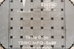
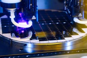
TSMC's System-on-Wafer Platform Goes 3D: CoW-SoW Stacks Up the Chips
TSMC has been offering its System-on-Wafer integration technology, InFO-SoW, since 2020. For now, only Cerebras and Tesla have developed wafer scale processor designs using it, as while they have...
2 by Anton Shilov on 4/26/2024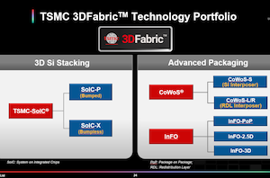
TSMC: We Want OSATs to Expand Their Advanced Packaging Capability
Almost since the inception of the foundry business model in the late 1980s, TSMC would produce silicon. In contrast, an outsourced semiconductor assembly and test (OSAT) service provider would...
2 by Anton Shilov on 10/16/2023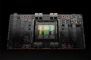
TSMC: Short Supply of HPC GPUs to Persist for 1.5 Years
The reports about an insufficient supply of compute GPUs used for artificial intelligence (AI) and high-performance computing (HPC) servers became common in recent months as demand for GPUs to...
6 by Anton Shilov on 9/7/2023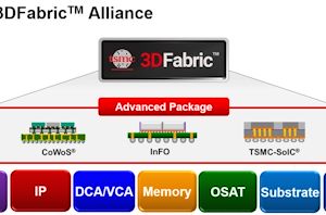
TSMC to Build $2.87 Billion Facility For Advanced Chip Packaging
TSMC on Tuesday announced plans to construct a new advanced chip packaging facility in Tongluo Science Park. The company intends to spend around $2.87 billion on the fab that...
3 by Anton Shilov on 7/25/2023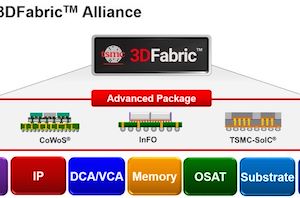
TSMC Opens Advanced Backend Packaging Fab for AI and HPC Products
TSMC on Friday formally opened its Advanced Backend Fab 6 facility, which it will be using to expand the company's capacity for building high-end, multi-chiplet products. The facility is...
1 by Anton Shilov on 6/9/2023
TSMC Forms 3DFabric Alliance to Accelerate Development of 2.5D & 3D Chiplet Products
Currently the majority of high-end processors are monolithic, but design methodologies are slowly but surely shifting to multi-chiplet modules as leading-edge fabrication technologies get more expensive to use. In...
9 by Anton Shilov on 10/27/2022
As HPC Chip Sizes Grow, So Does the Need For 1kW+ Chip Cooling
One trend in the high performance computing (HPC) space that is becoming increasingly clear is that power consumption per chip and per rack unit is not going to stop...
40 by Anton Shilov on 6/27/2022
TSMC Q1 2021 Process Node Revenue: More 7nm, No More 20nm
This week TSMC has disclosed its full quarterly financial results for Q1 2021. In those results the company often explains where the revenue demand is for its technologies, and...
40 by Dr. Ian Cutress on 4/15/2021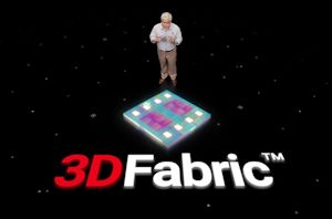
3DFabric: The Home for TSMC’s 2.5D and 3D Stacking Roadmap
Interposers. EMIB. Foveros. Die-to-die stacking. ODI. AIB.TSVs. All these words and acronyms have one overriding feature – they are all involved in how two bits of silicon physically connect...
9 by Dr. Ian Cutress on 9/2/2020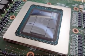
2023 Interposers: TSMC Hints at 3400mm2 + 12x HBM in one Package
High-performance computing chip designs have been pushing the ultra-high-end packaging technologies to their limits in the recent years. A solution to the need for extreme bandwidth requirements in the...
35 by Andrei Frumusanu on 8/25/2020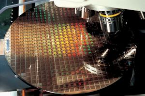
TSMC’s Version of EMIB is ‘LSI’: Currently in Pre-Qualification
Whilst process node technologies and Moore’s Law are slowing down, manufacturers and chip designers are looking to new creative solutions to further enable device and performance scaling. Advanced packaging...
19 by Andrei Frumusanu on 8/25/2020
TSMC Teases 12-High 3D Stacked Silicon: SoIC Goes Extreme
I’ve maintained for a couple of years now that the future battleground when it comes to next-generation silicon is going to be in the interconnect – implicitly this relies...
15 by Dr. Ian Cutress on 8/25/2020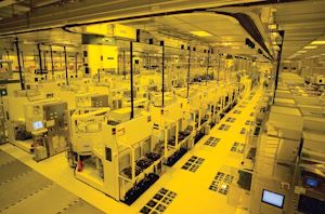
TSMC & Broadcom Develop 1,700 mm2 CoWoS Interposer: 2X Larger Than Reticles
With transistor shrinks slowing and demand for HPC gear growing, as of late there has been an increased interest in chip solutions larger than the reticle size of a...
18 by Anton Shilov on 3/4/2020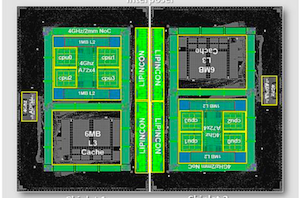
Arm & TSMC Showcase 7nm Chiplet, Eight A72 at 4GHz on CoWoS Interposer
Arm and TSMC this week unveiled their jointly developed proof-of-concept chip that combines two quad-core Cortex-72-based 7 nm chiplets on TSMC’s Chip-on-Wafer-on-Substrate (CoWoS) interposer. The two chips are connected...
26 by Anton Shilov on 9/27/2019


