Intel Broadwell Architecture Preview: A Glimpse into Core M
by Ryan Smith on August 11, 2014 12:01 PM ESTBroadwell CPU Architecture
We’ll kick off our look at Broadwell-Y with Broadwell’s CPU architecture. As this is a preview Intel isn’t telling us a great deal about the CPU at this time, but they have given us limited information about Broadwell’s architectural changes and what to expect for performance as a result.
With Broadwell Intel is at the beginning of the next cycle of their tick-tock cadence. Whereas tock products such as Haswell and Sandy Bridge designed to be the second generation of products to use a process node and as a result are focused on architectural changes, tick products such as Ivy Bridge and now Broadwell are the first generation of products on a new process node and derive much (but not all) of their advantage from manufacturing process improvements. Over the years Intel has wavered on just what a tick should contain – it’s always more than simply porting an architecture to a new process node – but at the end of the day Broadwell is clearly derived from Haswell and will be taking limited liberties in improving CPU performance as a result.
| Intel's Tick-Tock Cadence | |||||
| Microarchitecture | Process Node | Tick or Tock | Release Year | ||
| Conroe/Merom | 65nm | Tock | 2006 | ||
| Penryn | 45nm | Tick | 2007 | ||
| Nehalem | 45nm | Tock | 2008 | ||
| Westmere | 32nm | Tick | 2010 | ||
| Sandy Bridge | 32nm | Tock | 2011 | ||
| Ivy Bridge | 22nm | Tick | 2012 | ||
| Haswell | 22nm | Tock | 2013 | ||
| Broadwell | 14nm | Tick | 2014 | ||
| Skylake | 14nm | Tock | 2015 | ||
All told, Intel is shooting for a better than 5% IPC improvement over Haswell. This is similar to Ivy Bridge (4%-6%), though at this stage in the game Intel is not talking about expected clockspeeds or the resulting overall performance improvement. Intel has made it clear that they don’t regress on clockspeeds, but beyond that we’ll have to wait for further product details later this year to see how clockspeeds will compare.
To accomplish this IPC increase Intel will be relying on a number of architectural tweaks in Broadwell. Chief among these are bigger schedulers and buffers in order to better feed the CPU cores themselves. Broadwell’s out-of-order scheduling window for example is being increased to allow for more instructions to be reordered, thereby improving IPC. Meanwhile the L2 translation lookaside buffer (TLB) is being increased from 1K to 1.5K entries to reduce address translation misses.
The TLBs are also receiving some broader feature enhancements that should again improve performance. A second miss handler is being added for TLB pages, allowing Broadwell to utilize both handlers at once to walk memory pages in parallel. Otherwise the inclusion of a 1GB page mode should pay off particularly well for servers, granting Broadwell the ability to handle these very large pages on top of its existing 2MB and 4K pages.
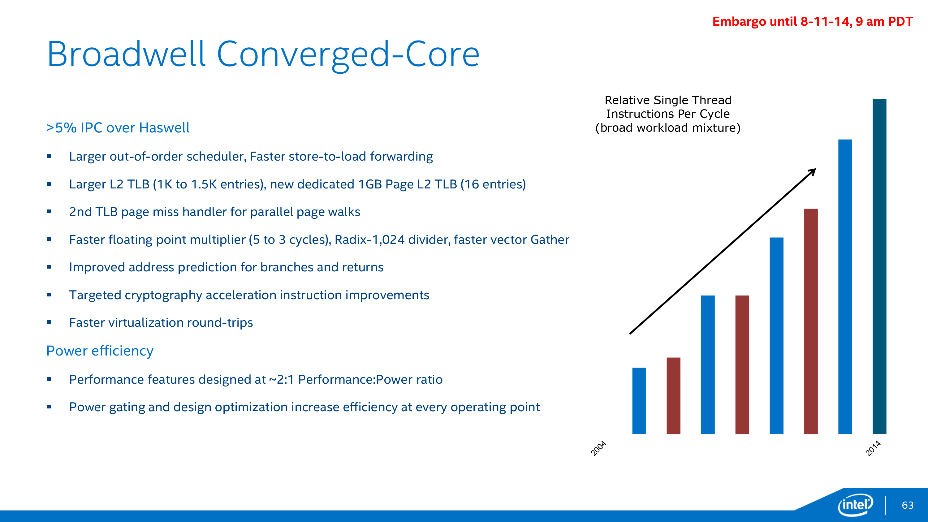
Meanwhile, as is often the case Intel is once again iterating on their branch predictor to cut down on missed branches and unnecessary memory operations. Broadwell’s branch predictor will see its address prediction improved for both branches and returns, allowing for more accurate speculation of impending branching operations.
Of course efficiency increases can only take you so far, so along with the above changes Intel is also making some more fundamental improvements to Broadwell’s math performance. Both multiplication and division are receiving a performance boost thanks to performance improvements in their respective hardware. Floating point multiplication is seeing a sizable reduction in instruction latency from 5 cycles to 3 cycles, and meanwhile division performance is being improved by the use of an even larger Radix-1024 (10bit) divider. Even vector operations will see some improvements here, with Broadwell implementing a faster version of the vector Gather instruction.
Finally, while it’s not clear whether these will be part of AES-NI or another instruction subset entirely, Intel is once again targeting cryptography for further improvements. To that end Broadwell will bring with it improvements to multiple cryptography instructions.
Meanwhile it’s interesting to note that in keeping with Intel’s power goals for Broadwell, throughout all of this Intel put strict power efficiency requirements in place for any architecture changes. Whereas Haswell was roughly a 1:1 ratio of performance to power – a 1% increase in performance could cost no more than a 1% increase in power consumption – Broadwell’s architecture improvements were required to be at 2:1. While a 2:1 mandate is not new – Intel had one in place for Nehalem too – at the point even on the best of days meaningful IPC improvements are hard to come by at 1:1, never mind 2:1. The end result no doubt limited what performance optimizations Intel could integrate into Broadwell’s design, but it also functionally reduces power requirements for any given performance level, furthering Intel’s goals in getting Core performance in a mobile device. In the case of Broadwell this means Broadwell’s roughly 5% performance improvement comes at a cost of just a 2.5% increase in immediate power consumption.
With that said, Intel has also continued to make further power optimizations to the entire Broadwell architecture, many of which will be applicable not just to Core M but to all future Broadwell products. Broadwell will see further power gating improvements to better shut off parts of the CPU that are not in use, and more generalized design optimizations have been made to reduce power consumption of various blocks as is appropriate. These optimizations coupled with power efficiency gains from the 14nm process are a big part of the driving force in improving Intel’s power efficiency for Core M.


158 Comments
View All Comments
crispbp04 - Monday, August 11, 2014 - link
Intel has something impressive in the works with Broadwell (at least on paper). I can't wait to get a Broadwell based Surface Pro. Assuming that Microsoft improves an already impressive hardware design from the sp3, the Broadwell iteration will likely be my next computer purchase.frostyfiredude - Monday, August 11, 2014 - link
I have a feeling SP4 will be fundamentally the same design as SP3 save for minor tweaks and improvements. SP3 was clearly designed for a processor with the kind of power profile Broadwell is set to deliver rather than the current Haswell profile. It will be interesting to see which set of SKUs Microsoft will put in the SP4, Core M or Broadwell ULT. Core M has a number of obvious benefits for power and area efficiency, but will it be powerful enough for their market with some features reduced from Haswell and Boradwell ULT.MonkeyPaw - Monday, August 11, 2014 - link
Pure speculation, but I think Intel might already be giving MS premium bins of Haswell for SP3, because SP3 is the only device to date to actually show off the ability to run premium Intel CPUs in a tablet format. Sure, MBA looks great, but SP3 took it to the next level.That said, I doubt that MS will use Core M in SP4, for the same reason we don't have Haswell-Y in SP3 (at least at the high end). It will probably be a step back in processing power to use one.
frostyfiredude - Tuesday, August 12, 2014 - link
Do we know what wattage the Broadwell ULT and Core M chips will be targeting? 15W TDP is clearly too high for the SP3 to handle so moving all SP4 chips to 11.5W like the current Haswell Y looks quite plausible at the moment, it just seems to be a matter of which version of Broadwell will have the 11.5W TDP.Samus - Wednesday, August 13, 2014 - link
15W is only a problem in SP3 to people who use it like a high performance computer (24x7 full load applications) but for general purpose use it barely warms up. We have people running Lightroom 8 hours a day on these things and like the Surface 2's (which I still have) they never got "hot" or "loud".That said, someone in the office infected their SP3 with some malware a few weeks ago (they literally owned the tablet not even 24 hours) and when they handed it to me, it was VERY hot with the fans whirling. Some 800kb task was using 100% of their CPU doing who knows what...at first I thought it was Cryptolocker but it turned out to be retrying a network connection. This was an i5 model, however, and it didn't seem to be throttling. The i3 will presumable run cooler, even at the same TDP.
What people need to keep in mind is these are mobile devices.
IntelUser2000 - Wednesday, August 13, 2014 - link
Broadwell ULT: 15WCore M(previously Broadwell-Y): 4.5W
vlad0 - Friday, August 15, 2014 - link
Isn't the core i3 version of the sp3 based on a Y series chip ?bebimbap - Monday, August 11, 2014 - link
agreed, Broadwell, and skylake will be vast improvements to PCs in general. Intel's Broadwell-Y announcement is all about "small, cool, efficient" while the recent FX-9590 seems more about "big, hot, gluttony" similar to the David vs Goliath story, the interesting part was the small one besting the big one. Ironically Intel is the bigger company. Hopefully AMD's new A1100 pans out as I don't want another Comcast, Microsoft, De Beers or Luxottica.wurizen - Monday, August 11, 2014 - link
well, if amd was as agressive as intel in shrinking dies or whathaveyou, then an AMD FX chip will probably be toe-to-toe to an intel i7-4930k or whatever the 6-core enthusiast intel chip is labeled. and not even die shrinks, but, also aggressive in producing a $500 cpu. imagine that. and you'd probably see an a10-7850k performance in a laptop by now. but, AMD seems content is sitting back and letting the other company do all the work, creating a path. as long as AMD doesn't completely die out, it's fine. we just need an alternative and AMD is the only one. so, go AMD. don't worry about broadwell. build it and we will come. be a niche. convert future x99 users to a future AMD product. and start from there.StevoLincolnite - Monday, August 11, 2014 - link
Except AMD can't be aggressive at shrinking dies.For one, die-shrinks costs money... For fab contracts, man-hours, research and possibly buying technology from other companies such as IBM.
AMD can't aggressively shrink dies anyway, they are at the mercy of fabrication companies like TSMC and Global Foundries, so what they can produce is limited to what they provide.
Intel has always been ahead of the industry in fabrication, the only way AMD can beat Intel is through something ground breaking (Like moving away from silicon?) or if Intel drops the ball, like they did with Netburst.
Or, AMD buys a fab company who is far ahead of Intel, which simply isn't going to happen.
Otherwise they can only compete on price and using an older more mature fabrication process allows them to do just that as the chips are much cheaper to produce, they just need to provide "Good enough" performance to mostly stay relevant, which the FX doesn't really do.