ASUS CUV266 Socket-370 Apollo Pro 266 ATX
by Mike Andrawes on April 18, 2001 12:50 AM EST- Posted in
- Motherboards
ASUS: The King of Overclocking
Besides being one of the largest OEM manufacturers, ASUS is also one of the favorites for hardware enthusiasts thanks to their products’ great stability and overclocking options. While they have been “one upped” at times by other manufacturers, such as ABIT, they have been doing their best to pick up the slack recently, and the CUV266 definitely puts ASUS right back at the top.
Following what has almost become “tradition,” ASUS allows both jumperless overclocking and overclocking by dipswitches. If you set the jumpers on the motherboard to jumperless mode, you will be able to adjust the FSB from inside the BIOS. Since most Intel chips are multiplier locked (engineering samples are the exception), it is very important to have a wide range of FSB speeds to maximize overclocking potential. ASUS did just that by providing 1MHz increments for the FSB between 66 and 193MHz. The PCI and AGP ratios are adjusted automatically so that these bus speeds are as close as possible to their default values of 33 and 66MHz, respectively.
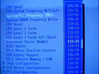
FSB speeds available in the BIOS in 1MHz increments.
In front of the fourth and fifth PCI slots, there is a set of dipswitches for changing the FSB speed. The available speeds are silk screened on the PCB as well, so you should be able to adjust the settings without consulting the manual. Unfortunately, not all the FSB speeds are available via the dipswitches, so BIOS overclocking is the better and easier way to go in most cases.
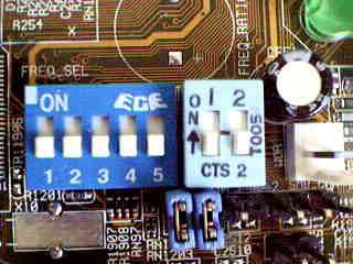
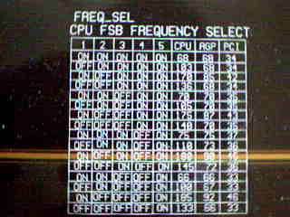
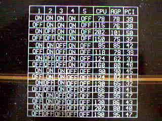
Dipswitches controlling the FSB speeds.
ASUS also put in a reasonable range of CPU core voltages, between 1.65 and 1.95V in 0.05V increments, to make the system more stable under overclocking situations. This is done within the BIOS and you can monitor the actual voltage that is being output in the BIOS as well. Besides the CPU core voltage, you can also read three temperatures and three fan speeds in the BIOS. The interesting part of the ASUS’s hardware monitoring setup is that they decided not to use the integrated hardware monitoring capabilities of the VIA 8233 South Bridge, but instead went with a custom ASIC, the AS99127F. The board offers three fan headers, one for the CPU’s HSF unit and two for chassis fans.
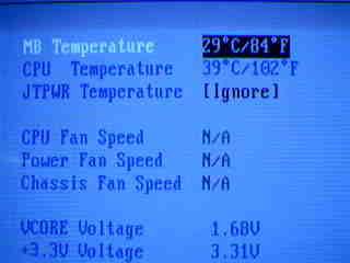
Hardware monitor in the BIOS.
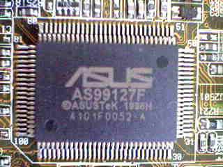
ASUS ASIC for hardware monitoring.
I/O voltage tweaking can also be very important in maintaining the stability of an overclocked system. This setting is available on the CUV266 through a set of jumpers on the board. The voltages available are 2.65V, 2.75V, and 2.9V, where 2.65V is the default setting. Notice that these voltages are much lower than the I/O voltages found on most other boards. This is due to the fact that DDR SDRAM runs at a lower 2.5V, while traditional SDRAM runs at 3.3V.
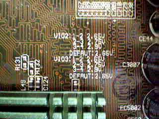
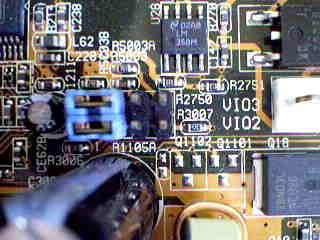
I/O voltage settings.
The CUV266 also offers a variety of options for memory tweaking. However, keep in mind that since DDR SDRAM is still in its infancy compared to traditional SDR SDRAM, current DDR memory may or may not be as tweakable as we’ve come to expect from SDR SDRAM. In our tests, pushing the memory settings wasn’t the best idea and readily degraded the stability of the test system.
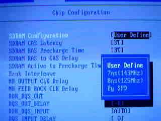
Memory tweaking options in the BIOS.
Overclocking on the CUV266 turned out to be quite good. With the CPU core and I/O voltages set to default and memory timings set to CAS2.5 with no memory interleaving, we were able to push the FSB of the system to 139MHz without any penalties on the stability of the system. With today’s Socket-A motherboards routinely pushing 150+ MHz FSB speeds, this seems extremely low. It currently appears that we’re limited by the DDR memory interface - whether the modules we’re using or something in the chipset is imposing that limitation remains to be seen. We’ll continue testing, and as soon as we know where the limitation is, we’ll let you know.


0 Comments
View All Comments