Original Link: https://www.anandtech.com/show/4019/a-brief-look-at-upcoming-asus-p67-motherboards
A brief look at upcoming ASUS P67 Motherboards
by Ian Cutress on November 14, 2010 1:22 PM EST- Posted in
- Motherboards
- Asus
- News
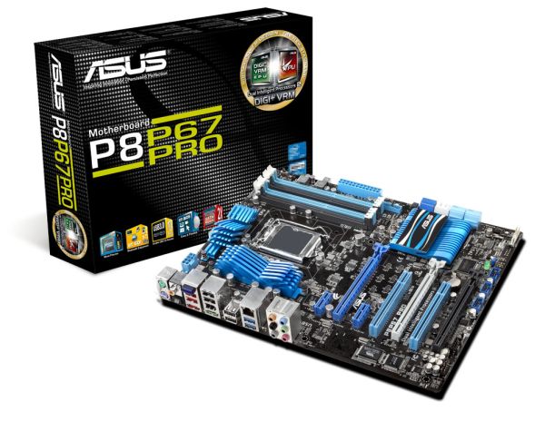
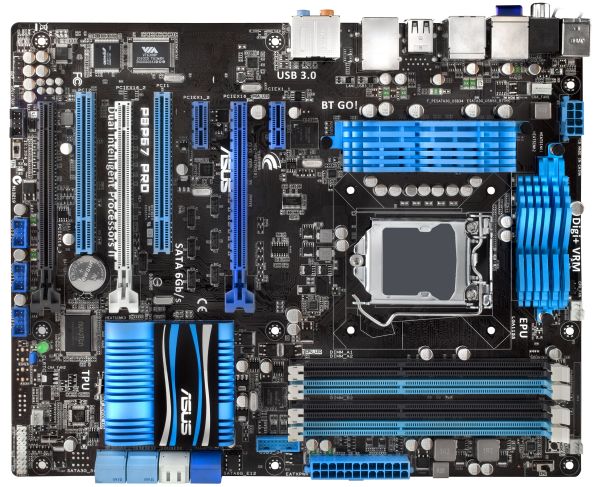
On first inspection, this board’s aesthetic blue and black livery is impressive. The big blue heatsinks on the VRM, while looking good with a large surface area, intrude slightly on the socket, potentially resulting in restricting the orientation of high end air coolers.
Among the standard features you’d expect on a P67, such as the four dual-channel DDR3 slots, and four SATA 3Gb/s with two SATA 6Gb/s supported by the chipset, there is another two SATA ports, but it is unclear if these are for the RAID, 3Gb/s or 6Gb/s, or how they are powered, as they are not labelled and the chipset heatsink covers quite a bit. Two NEC controllers give two USB 3.0 ports on the back panel, and the possibility for another two via a header on the board connectable to the case, or to an ASUS USB 3.0 port box (as shown in the P67 Deluxe images). The Sandy Bridge platform on P67 relies on discrete graphics only, and as such there are no video out connectors on the back panel, but two PCIe x8 slots on the board itself (or one PCIe x16 if only one card is used). There is another PCIe slot available, presumably x4, for non-GPU duties.
The back panel itself is fairly standard – dual PS/2 ports for keyboard and mouse, S/PDIF out, six USB 2.0 ports, two USB 3.0 ports, two eSATA connectors, firewire, 5.1 audio and gigabit Ethernet. Also of note is the Bluetooth receiver, which is a nice addition, but the lack of a second gigabit Ethernet port, which by now we feel should be a staple on all high end boards and any board with the ‘Pro’ moniker, isn’t too pleasing.
On the board, we see two switches for TPU (TurboV Processing Unit) and EPU (Energy Processing Unit). The TPU is designed to monitor FET thermal temperatures, while the EPU will moderate power appropriately across the VRMs. Both can be turned on and off by the onboard switches, and presumably in the BIOS as well.
Speaking of switches, we’re disappointed that ASUS have not put easy-to-use power and reset switches on the Pro. Sure, not everyone needs them, but they are a nice addition rather than having to short two front panel pins with a screwdriver (when slightly tired, it’s never a good idea to accidentally short the wrong pins, unless you want to see some sparks).
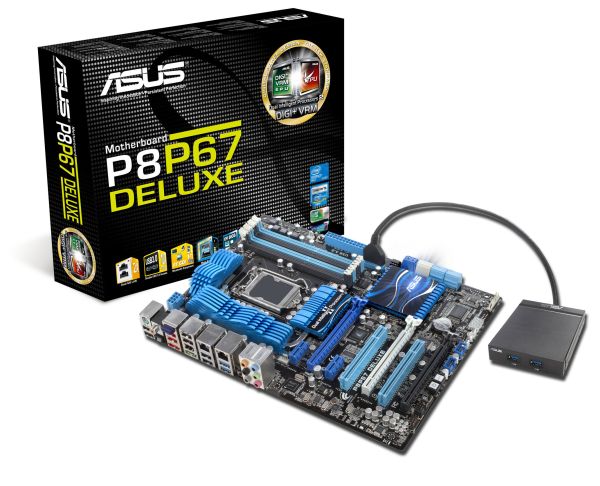
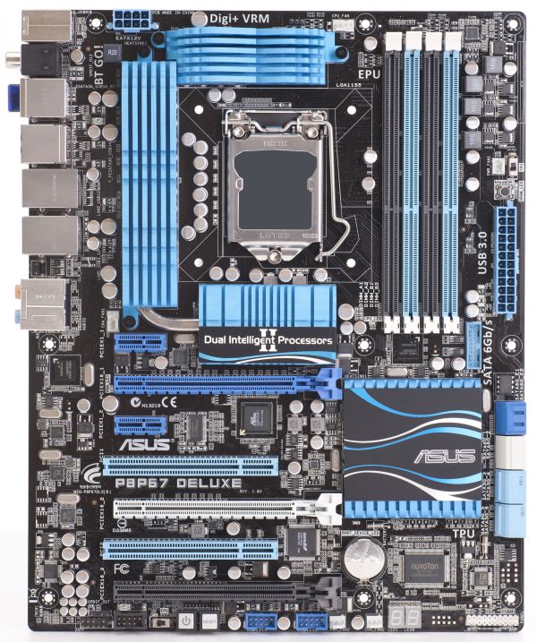
The Deluxe has more of the features we expected from the Pro board. In a similar design, we see power and reset switches on the board, dual gigabit Ethernet and double-digit debugging LEDs.
The extended VRM heatsink cooling is the most obvious visual change over the Pro, despite the fact that the Pro and the Deluxe both have only one 8-pin 12V connector, which suggests that ASUS have shelled out a few more reddies on the VRM for the socket on the Deluxe. Whether that plays out to any performance gain, or a raise in the performance ceiling, we’ll find out in due course.
The main back panel change, apart from the presence of dual gigabit Ethernet, is the combination PS/2 mouse and keyboard port, and the CMOS clear button. The button itself is recessed slightly behind the 5.1 audio and the USB ports on either side, so in order to press it, you really have to be searching for it. Or if your cat decides it’s a toy on the back panel and accidentally claws it with some force.
Other additions/changes of note is the PLX chip between the first PCIex16 slot and the first PCI slot, and the relocation of the bridging USB2.0/3.0 to SATA ASMedia chip to a more central location next to the battery. The Deluxe, like the Pro, has eight SATA ports in total, but these are labelled, and shows four SATA 3Gb/s (labelled 3, 4, 5 and 6), two SATA 6Gb/s, and two more SATA 6Gb/s, designated ‘E’. This raises a couple of questions – what happened to SATA 3Gb/s which are labelled 1 and 2? If the 6Gb/s ‘E’ designation is for eSATA, why are the back-panel eSATA ports labelled 3Gb/s?
Obviously, expect the Deluxe to retail at a high price than the Pro. How much more, we don’t know yet, and ASUS is keeping that info to themselves.
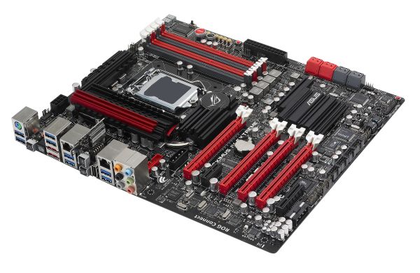
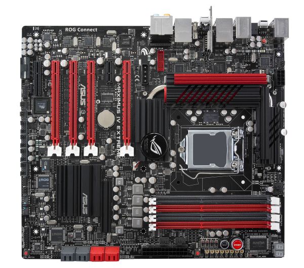
The first board in the Sandy Bridge series with the Republic of Gamers moniker is the Maximus IV Extreme. This motherboard looks jam-packed with features, and we’d expect nothing less from a ROG product.
The red and black aside, ASUS are attempting to pushing the boat out for overclockers. Of immediate notice is beside the dual-channel DDR3 slots – alongside the power and reset buttons are a set of four switches, designed to enable and disable the PCIe slots as required. Beside these are a set of eight voltage readout points, allowing the monitoring of the various DRAM, NF200, PCH and the CPU voltages across the board. A switch is also present labelled ‘LN2_MODE’, which offers various questions as to what it does, but we suspect at least one of these features is to remove the overcurrent protection when the processor is under liquid nitrogen. One point of humorous mention is that there are three LEDs next to the DDR3 slots, one of them labelled ‘DDR_CRAZY’.
The Maximus IV operates a dual BIOS system, as directed by the two chips labelled BIOS1 and 2, and the BIOS switch in the bottom corner of the board. The dual-digit debugging LEDs, as we would expect, are present also.
Surprisingly, only one 8-pin 12V connector is on the board, which is somewhat odd if the board has a liquid nitrogen mode and power needs to be pumped into the CPU. In terms of extra power for the PCIe slots, a 4-pin molex connector is provided where a PCIe x1 slot is found on the Pro and Deluxe boards. The board is obviously built for multiple graphics card use and overclocking, but as the P67 chipset is designed to only hold 16 PCIe lanes for graphics card usage – ASUS have added an NF200 chip to increase the amount of available lanes, presumably to 32 for an x16/x16 or x16/x8/x8 configuration. On previous motherboard generations, the NF200 chip accounts for a 1-2% loss in performance when the lanes are not fully utilised versus native support, as well as few more extra monies and power usage, thus all the GPU lanes need to be used to get the most out of the board – this is what the consumer is paying for, after all.
The back panel offers the usual myriad of USB 2.0 / 3.0, firewire, eSATA, 5.1 audio, PS/2 and dual Ethernet connectors, but the use of a mini-PCB perpendicular to the motherboard to supply the board with Bluetooth and what looks like a ROG connect switch is interesting. Also of note is an NEC/TOKIN Proadlizer film capacitor, similar to that used on some GPUs, directly next to the socket – presumably to provide more stable power to the socket.
Apart from the possible results this motherboard may or may not achieve, one thing is certain – it will be costing the consumer a pretty penny. No doubt we will have one in to test at some point, and we’ll keep our ears to the ground on other manufacturer’s flagship Sandy Bridge boards.

