Original Link: https://www.anandtech.com/show/15877/intel-hybrid-cpu-lakefield-all-you-need-to-know
The Intel Lakefield Deep Dive: Everything To Know About the First x86 Hybrid CPU
by Dr. Ian Cutress on July 2, 2020 9:00 AM EST
For the past eighteen months, Intel has paraded its new ‘Lakefield’ processor design around the press and the public as a paragon of new processor innovation. Inside, Intel pairs one of its fast peak performance cores with four of its lower power efficient cores, and uses novel technology in order to build the processor in the smallest footprint it can. The new Lakefield design is a sign that Intel is looking into new processor paradigms, such as hybrid processors with different types of cores, but also different stacking and packaging technologies to help drive the next wave of computing. With this article, we will tell you all you need to know about Lakefield.
Part Smartphone, Part PC
When designing a processor, there are over a thousand design choices to be made. The processor can be built to tackle everything, or it can be aimed at a niche. For high performance computing, there might be a need for a high power, high performance design where cooling is of no consideration – compare that to a processor aimed at a portable device, and it needs to be energy efficient and offer considerable battery life for a fixed battery size. There is also the cost of designing the product, how much to invest into research and development, how many units are expected to sell, and thus how many should be produced and what size the product should be. What the price range of the target market is can be a huge factor, even before putting pen to paper.
This is all why we have big multi-core processors with lots of compute acceleration in servers, more moderate power and core counts in home machines that focus on single core performance and user experience, and why smartphone processors have to physically fit into a small design and offer exceptional battery life.
Laptop processors have always sort of fit into the middle of the PC and smartphone markets. Laptop users, especially professionals and gamers, need the high performance that a desktop platform can provide, but road warriors need something that is superbly efficient in power consumption, especially at idle, to provide all-day battery life as if they were on a good smartphone. Not only this, but the more energy efficient and the smaller the footprint of the processor and its features, the thinner and lighter the laptop can be, offering a premium design experience.
As a result, we have seen the ultra-premium notebook market converge from two directions.
From the top, we have AMD and Intel, using their laptop processor designs in smaller and smaller power envelopes to offer thin and light devices with exceptional performance and yet retain the energy efficiency required for battery life. For the most premium designs, we see 12-15+ hours of laptop battery life, as well as very capable gaming.
From the bottom, we have Qualcomm, building out its high-performance smartphone processor line into larger power envelopes, in order to offer desktop-class performance with smartphone-class connectivity and battery life. With the designs using Qualcomm’s processors, a user can very easily expect 24+ hours of battery life, and with regular office use, only charge the system once every couple of days. Qualcomm still has an additional barrier in software, which it is working towards.
Both of these directions converge on something in the middle – something that can offer desktop-class performance, 24hr+ battery life, capable gaming, but also has a full range of software support. Rather continue with trying to bring its processors down to the level it requires, Intel has decided to flip its traditional processor paradigm upside down, and build a smartphone-class processor for this market, matching Qualcomm in its bottom up approach while also looking into novel manufacturing techniques in order to do so.
This processor design is called ‘Lakefield’.
Lakefield at the Core, and the Atom
For the past two decades, Intel has had two different types of x86 CPU design.
The Big ‘Core’ CPU
Intel calls its high power/high performance x86 design the ‘Core’ family. This can make it very confusing, to differentiate between the general concept of a processor core and a ‘Core’-based processor core.
Over the years, Core-based processor cores have been designed for power envelopes from low-power laptops all the way up to the beefiest of servers. The Core line of processor cores implement more complex logic in order to provide additional acceleration, at the expense of physical size and power.
The Small ‘Atom’ CPU
The second type of x86 design from Intel is its more energy efficient implementation, called ‘Atom’. With the Atom cores, Intel simplifies the design in order to maximise efficiency for a given power or a given performance. This makes the design smaller, cheaper to manufacturer, but has a lower peak performance than the Core design. We typically see Atom designs in power restricted scenarios where performance is not critical, such as IoT, or low cost laptop designs.
Where Core Meets Atom
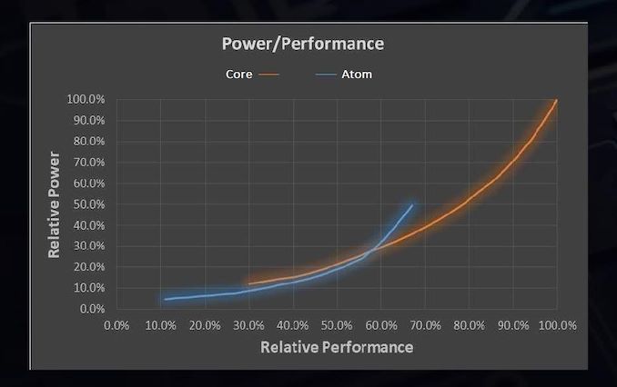
Normally we characterise a processor core design in terms of this power and performance. Due to the variation in the design, we see where some designs work best, at various points for a given power or for a given performance. In the case of Intel’s latest generation of Core and Atom hardware, it looks something like this, if we compare one thread against one thread:
From this graph, which measures Performance on the bottom axis and power on the side axis, there is a crossover point where each design makes the best sense. When the demand for performance is below 58%, the Atom design is the most power efficient, but above 58% then a Core design is preferred.
Homogenous CPUs (all the same) vs
Heterogeneous CPUs (mix of different)
Now in modern processors, especially in laptops, desktops, and servers, we only experience one type of core design. We either have all Core or all Atom, and the performance is designed to scale within those homogeneous designs. It becomes a simple curve to navigate, and when more parallel performance is required, more of those types of cores are fired up to serve the needs of the end user. This has been the case for these markets for the last 30-50 years.
The smartphone space, for the last decade, has been taking a different approach. Within the smartphone world, there are core designs listed as ‘big’ and core designs listed as ‘little’, in the same way that Intel has Core and Atom designs.
These smartphone processors combine numbers of big cores with numbers of small cores, such that there is an intrinsic benefit to running background tasks on the little cores, where efficiency is important, and user experience related elements on the big cores, where latency and performance is important.
The complexity of such a heterogeneous smartphone-like design has many layers. By default most items will start on the little cores, and it is up to either the processor or the operating system to identify when the higher performance mode during a user experience moment is needed. This can be tricky to identify.
Then also comes the matter when a workload has to actually move from one type of core to the other, typically in response to a request for a specific level of performance – if the cores are designed significantly different, then the demands on the memory can likely increase and it is up to the operating system to ensure everything works as it should. There is also an additional element of security, which is a larger topic outside of the scope of this article.
Ultimately building a design with both big cores and little cores comes down a lot to what we call the scheduler. This is a program inside the operating system that manages where different background processes, user experience events, or things like video editing and games, get arranged. The smartphone market has been working on different types of schedulers, and optimizing the designs, for over a decade as mentioned. For the land of Intel and AMD, the push for heterogeneous schedulers has been a slow process by comparison, and it becomes very much a chicken and egg problem – there is no need for an optimized heterogeneous scheduler if there is never a heterogeneous processor in the market.
So why bring all this up?
Lakefield is the first x86 heterogeneous processor.
In its marketing, Intel calls this a ‘hybrid’ CPU, and we will start to see logos identifying this as such. At the heart of its design, Lakefield combines one of the big Core designs with a cluster of four smaller Atom designs, all into one single piece of silicon. In normal x86 processor talk, this is essentially a ‘penta-core’ design, which will commonly be referred to as a 1+4 implementation (for one big core and four small cores).
Intel’s goal with Lakefield is to combine the benefits of the power efficient Atom core with the better user-experience elements provided by the more power hungry but better peak performing big Core. As a result, it sits in the middle of Intel’s traditional homogeneous designs which only contain one type of x86 design – somewhere above the ‘all Atom’ 0+4 design and somewhere below the ‘all Core’ 4+0 design (in actual fact, it’s closer to 0+4).
Based on our conversations with Intel, and the small demonstrations we have seen so far, the best way to consider the new Lakefield processor is to consider it similar to one of the older quad-core Atom processors, with the benefits of the single core performance of a big Core. The cluster of four smaller Atom CPUs will take care of the heavy lifting and parallel performance requests, because there are four of them, while the big Core will respond when the user loads an application, or touches the screen, or scrolls a web browser.
Being a new form of x86 hybrid CPU is not the only thing that Lakefield brings to the table.
Now, just for some form of clarification, we have already had some experience with these sorts of hybrid CPU designs on operating systems like Windows. Qualcomm’s Windows on Snapdragon laptops, like the Lenovo Yoga, use a 4+4 design with the Snapdragon smartphone chips, and Qualcomm has had to work extensively with Microsoft to develop an appropriate scheduler that can manage workloads between the different CPU designs.
The main difference to what Qualcomm has done and what Intel is doing with Lakefield is in software support – Qualcomm processors run ‘Arm’ instructions, while Intel processors run ‘x86’ instructions. Most Windows software is built for x86 instructions, which has limited Qualcomm’s effectiveness in penetrating the traditional laptop market. Qualcomm's design actually allows for ‘x86 translation’, however its scope is limited and there is a performance penalty, but is a work in progress. The point being is that while we have not had a hybrid CPU scheduler for Windows on an x86 system previously, there has been a lot of work put in by Microsoft to date while working with Qualcomm.
Visualising Heterogeneous CPU Designs
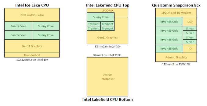
Here are some examples of mobile processors, from Intel and Qualcomm, with the cores in green. On the left is Intel's own Ice Lake processor, with four big cores. In the middle is Intel's Lakefield, which has two stacked silicon dies, but it's the top one that has one big core and four small ones. On the right is Qualcomm's Snapdragon 8cx, currently used in Windows on Snapdragon devices, which uses four performance cores and four efficiency cores, but also integrates a smartphone modem onboard.
In this article, over the following pages, we'll be looking at Intel's new Lakefield processor in detail, covering the new multi-core design, discussing chiplets and Intel's new die-to-die bonding technology called Foveros, the implications of such a design on laptop size (as well as looking at the publicly disclosed Lakefield laptops coming to market), die shots, supposed performance numbers, thermal innovations, and the future for Lakefield. Data for this article has come from our research as well as interviews with Intel's technical personnel and Intel's own presentations on Lakefield at events such as HotChips, Architecture Day, CES, IEDM, and ISSCC. Some information is dissected with helpful input from David Schor of Wikichip. We also cover some of Intel’s innovations with the scope of other semiconductor companies, some of which may be competitors.
A Stacked CPU: Intel’s Foveros
The previous designs of Intel, AMD and Qualcomm are what we call monolithic designs – everything on the processor happens on a single piece of physical silicon. When everything is on a single piece of silicon, it makes data management inside the processor a lot easier and simpler, it makes designing the processor a lot simpler, and manufacturing and assembly can be streamlined when only dealing with one physical element to the processor.
However, there have been moves in the industry to deviate from these single monolithic designs, as the benefits of trying something different are starting to offer beneficial points of differentiation within a product portfolio. It can lead to optimizations on different parts of the processor, it can be advantageous for cost reasons, and it also can expand silicon products beyond traditional manufacturing limits as well.
Monolithic vs Chiplets
You may be aware that recent AMD desktop processors are built on a ‘chiplet’ design. This is where multiple pieces of silicon are connected through wires in the green PCB in order to create a single ‘processor’. By using separate chiplets, each individual chiplet can either be focused on a single task (and be manufactured in the most efficient way for that task) or it can be a one of a repeated unit designed to scale out the compute performance.
For example, a processor core that contains logic circuits might aim for performance, and thus might require a very speed optimized layout. This has different manufacturing requirements compared to something like a USB controller, which is built to a series of specifications as per the USB standard.
Under a traditional monolithic regime, the single piece of silicon will use a singular manufacturing process that has to be able to cater for both situations – both the processor core logic and the USB controller. By having different parts of the overall design separated in different pieces of silicon, each one optimized for the best manufacturing scenario. This only works as long as the connectivity between the chips works, and it potentially enables a better mix of performance where you need it, and better efficiency (or cheaper cost) where you need it as well.
Of course, there are trade-offs: additional connectivity is required, and each chiplet needs to be able to connect to other chiplets – the total physical design area of the combined chiplets is often greater than what a single piece of silicon would offer because of these connectivity additions, and it could become costly to assemble depending on how many parts are involved (and if those parts are manufactured in different locations). Ultimately, if some chiplets are on an expensive manufacturing process, and some are on a cheaper manufacturing process, then we get the benefits of the expensive process (power, performance) without having to spend the money to build everything on that process, overall saving money.
One other benefit that a chiplet process can bring is total silicon size of the product. Standard monolithic silicon designs, due to the manufacturing process technologies we use today, have an upper bound of how big a single piece of silicon can be. By implementing chiplets, suddenly that upper limit isn’t much of a concern unless each chiplet reaches that limit - using multiple chiplets can give a total silicon area bigger than a single monolithic chip design. An example of this is AMD’s Rome CPUs, which total an area of over 1000 square millimetres, while the single largest monolithic silicon die is NVIDIA’s A100 GPU, coming in at 826 square millimetres.
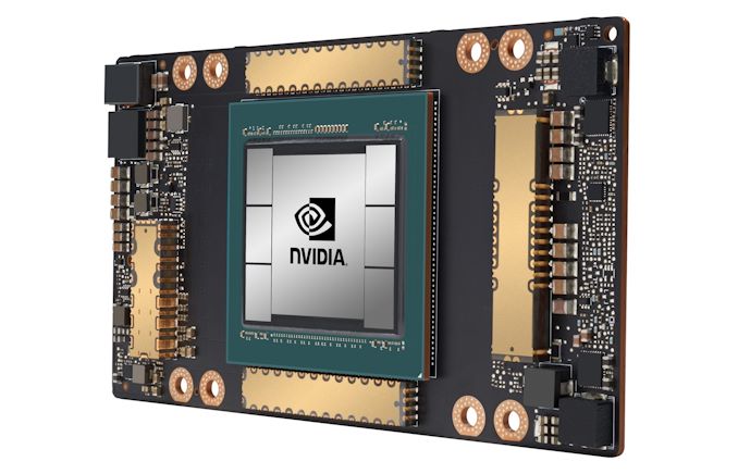
NVIDIA's A100 GPU, with one big monolithic die and six high bandwidth memory dies.
Already in Market: AMD Chiplets
To put this into context of a modern design, AMD’s Ryzen processors use one or more ‘compute chiplets’ combined with a single ‘peripheral’ chiplet (often called an IO die). The compute chiplets are built on TSMC’s high-performance 7nm manufacturing node which extracts peak performance and power from the design. The ‘peripheral’ chiplet, which is not so peak performance focused but more tuned to standards like SATA, PCIe and USB, can be built on a manufacturing node where efficiency is more important, and also the cost can be lower, such as GlobalFoundries’ cheaper 14nm manufacturing node. Put together, these chiplets form a singular product.
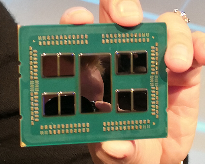
AMD's Rome with 1 big IO die and eight compute dies
AMD had to overcome a lot of hurdles to get here, such as developing a chip-to-chip connectivity standard (known as Infinity Fabric), managing the power of the connectivity, but also physical manufacturing, such as ensuring all the individual chiplets match the same height for the heatspreader and cooler that goes on top to be effective.
One of the benefits of AMD going this route, according to the company, is that it allows them to scale the parts of their design that are easiest to scale for performance (the compute cores), and also manage where they think the future of compute is going. The other big benefit is that total die size of one of AMD’s server CPUs is larger than what can be manufactured in a single piece of silicon.
This sort of chiplet based approach also lends people to believe that AMD could swap out a compute based chiplet for a graphics based chiplet, or an AI-focused chiplet, and thus AMD could in the future offer different variants of its products depending on customer requirements for different workloads that the organization might have.
Coming to Market: Intel Chiplets
For Lakefield, Intel also goes down the chiplet route. But instead of placing the chiplets physically alongside each other like AMD, the chiplets are stacked on top one another. This creates a physically smaller processor package in the x-y dimensions, which is a critical component for laptop and small form factor mobile designs that Lakefield is aiming towards.
This stacked design replaces the tradeoff of physical space for one of cooling. By placing two high-powered bits of silicon on top of each other, managing thermals becomes more of an issue. Nonetheless, the physically smaller floorplan (along with a design focused to embed more control into the processor) in the x-y directions helps build thinner and lighter systems.
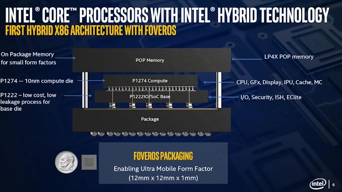
For the two stacked chiplets in the middle, the top chiplet is built on Intel’s high-performance 10nm+ manufacturing node and contains the 1+4 compute core configuration, as well as the graphics and the memory controller. The bottom chiplet contains the ‘peripheral’ components that are not as performance related, such as security controller, USB ports, and PCIe lanes. This is built on Intel’s cheaper 22nm manufacturing node.
Because this chiplet is on the bottom and has connections for power to pass through, Intel technically calls the lower chiplet an ‘active interposer’. An interposer is a term commonly used when chiplets are connected through a base piece of silicon, rather than through a green package PCB, because it allows communication between chiplets to be faster and more efficient, but it is a more expensive implementation.
What makes it an active interposer, rather than the passive interposers we have seen on some GPUs in recent years, is that it contains functional logic, such as the USB ports, the security, the chipset functions, and others. The passive interposers are just connection passthroughs, taking advantage of faster signaling. Active interposers include functional logic and have an associated power consumption that goes along with that.
The reason I bring this up is because there is some debate as to whether an active interposer is true 3D stacking as traditionally interpreted, or more akin to 2.5D stacking, which is what we commonly call a passive interposer. For those users who read more about Lakefield beyond AnandTech, you are likely to see both used.
Getting Stacked: DRAM and NAND vs Lakefield
The use of stacking is not necessarily new to the world of semiconductors. Both computer random access memory, such as DRAM, and storage components, such as NAND Flash, have implemented multiple layer technology for many years. What makes these elements different is the way they are stacked, plus also the power of the components involved.
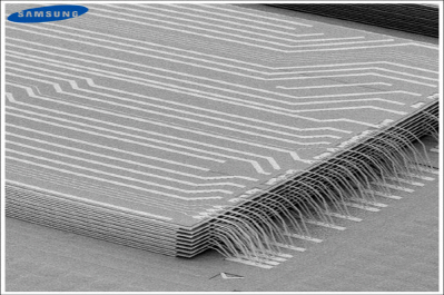
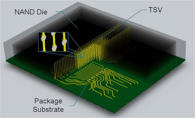
The two main ways of stacking silicon together are through simple wire bonding, where the layers are not directly connected, or with Through Silicon Vias (TSVs), which are akin to stacks running through the layers.
This is an image of Samsung’s NAND wire bonding technique, where multiple layers have separate connections to a base die. There is no direct connection between layers other than the act of physically coming together.
This is ‘Through Silicon Via’ (TSV) stacking, whereby each layer has a vertical channel that connects to the die above and below it. It allows for direct connection through the stack for fast access, which is useful when NAND has 64 or more layers. It can be quite difficult to do as well, but NAND manufacturers are experts in this methodology.
However, DRAM and NAND Flash are not the high-powered elements of a computer. Even the most dense memory configurations look to contribute single digit of milliwatts of power per layer when in use. Applying these techniques to high-powered computer chips is a bit more complex.
Stacking with Lakefield
What Intel is doing with Lakefield, with its stacking, is putting together multiple layers of high-performance compute into a single product. Also, while most DRAM and NAND Flash implementations stack silicon on top of each other, and then use external wire bonding or TSVs, to provide connectivity - for Intel’s Lakefield, the connectivity goes through the silicon, as with a traditional interposer (as mentioned above), and uses a die-to-die bonding to provide the communications.
Intel calls its stacking technology ‘Foveros’. It uses a novel design of die-to-die connectivity.
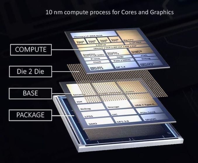
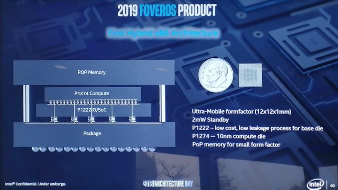
At the bottom is the base packaging material that connects all the signals going out into the system (power, USB, display). On top of this is the base silicon peripheral die, the active interposer, containing things like the USB control, storage control, security, and such.
Between the base silicon peripheral die and the top logic compute die is a method of connecting the two, in this case we have a solder ball array with a 50 micron pitch. This is essentially a ‘balls-on-balls’ technique, but with two silicon dies of different process node manufacturing techniques.
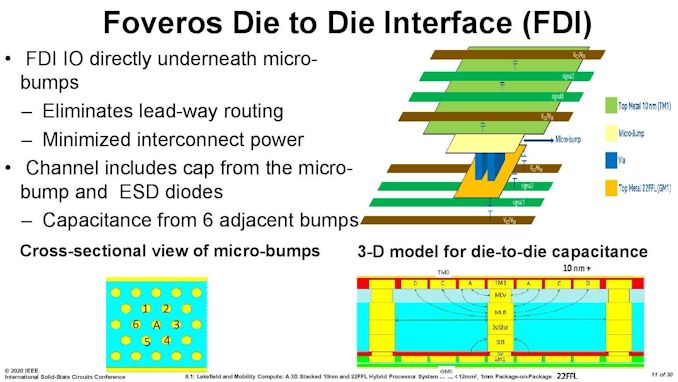
These connections will come in three flavors: structural, data, and power. Creating these bumps and ensuring they deliver what is intended is a hard problem – electrical issues, such as capacitance, and computational issues, such as maintaining a clock frequency, have to be managed, along with achieving targets in data rate bandwidth as well as power.
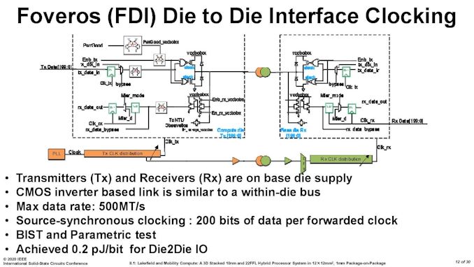
Here is the main introduction slide that Intel presented at the ISSCC conference regarding the die-to-die interface. Unfortunately these were the quality of the pictures as presented (the unreadable aspect ratios are also native to the presentation).
As mentioned, maintaining the clock coherency at speed and low power is a concern, and here’s what Intel did, with each connection operating at 500 mega-transfers per second. The key point on this slide is the power: 0.2 picojoules of energy consumed per bit transferred. If we extrapolate this out to a memory bandwidth of 34 GBps (maximum memory bandwidth of Lakefield), this equates to 54 millwatts of power for the data transfer.
0.2 pJ/bit is one of the benefits of keeping the transmission of the data ‘inside’ the silicon, but moving between the two layers. This is an order of magnitude better than the numbers quoted by AMD for its first generation EPYC server processors, which used data transfer links within the CPU package – AMD quoted 2 pJ/bit transfer by comparison.
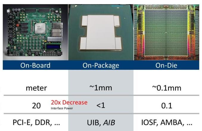
Here’s a slide from Intel’s 2018 Hot Chips talk about new data transfer and connectivity suggestions. On the left is the ‘on-board’ power transfer through a PCB, which runs at 20 pJ/bit. In the middle is on-package data transfer, akin to what AMD did with 1st Gen EPYC’s numbers, around 1-5 pJ/bit (depends on the technique), and then we get on-silicon data movement, which is more 0.1 pJ/bit. Intel’s Foveros die-to-die interconnect is most like the latter.
Lakefield: Top Die to Bottom Die
At the top is the compute die, featuring the compute cores, the graphics, and the display engines for the monitors.
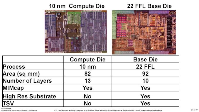
It might be easier to imagine it as the image above. The whole design fits into physical dimensions of 12 mm by 12 mm, or 0.47 inch by 0.47 inch, which means the internal silicon dies are actually smaller than this. Intel has previously published that the base peripheral interposer silicon is 92 mm2, and the top compute die is 82 mm2.
Compute Die
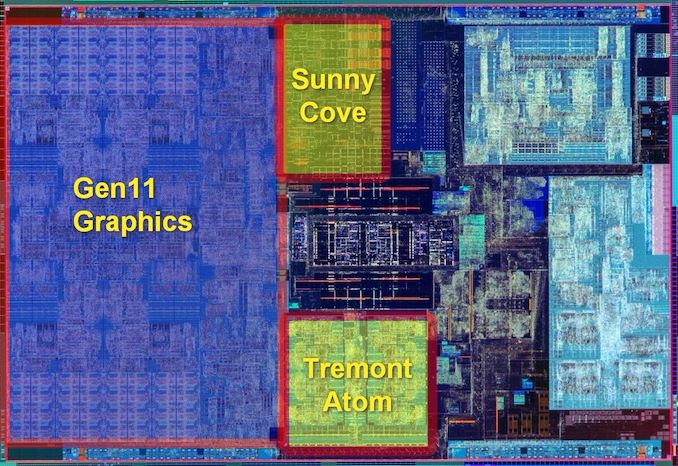
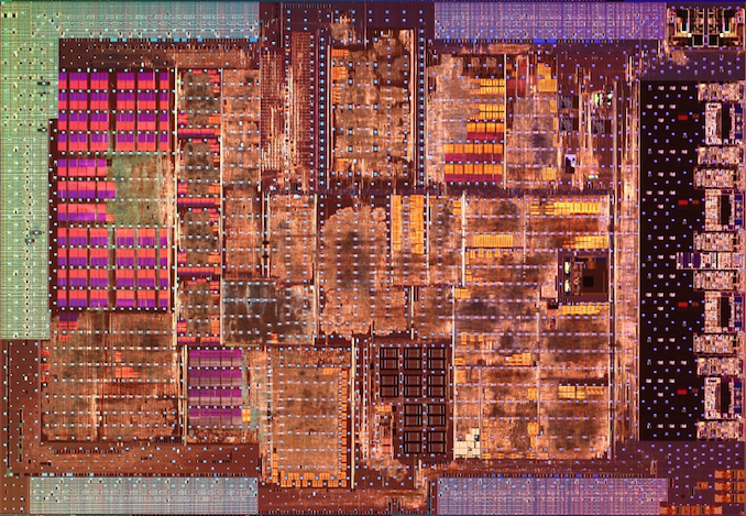
Where most of the magic happens is on the top compute die. This is the piece of silicon built on Intel’s most advanced 10+ nm process node and contains the big core, the small cores, the graphics, the display engines, the image processing unit, and all the point-to-point connectivity. The best image of this die looks something like this:
The big block on the left is the Gen 11 graphics, and is about 37% of the top compute die. This is the same graphics core configuration as what we’ve seen on Intel’s Ice Lake mobile CPUs, which is also built on the same 10+ process.
At the top is the single Sunny Cove core, also present in Ice Lake. Intel has stated that it has physically removed the AVX-512 part of the silicon, however we can still see it in the die shot. This is despite the fact that it can’t be used in this design due to one of the main limitations of a hybrid CPU. We’ll cover that more in a later topic.
At the bottom in the middle are the four Tremont Atom cores, which are set to do most of the heavy lifting (that isn’t latency sensitive) in this processor. It is worth noting the relative sizes of the single Sunny Cove core compared to the four Tremont Atom cores, whereby it seems we could fit around three Tremont cores in the same size as a Sunny Cove.
On this top compute die, the full contents are as follows:
- 1 x Sunny Cove core, with 512 KiB L2 cache
- 4 x Tremont Atom cores, with a combined 1536 KiB of L2 cache between them
- 4 MB of last level cache
- The uncore and ring interconnect
- 64 EUs of Gen11 Graphics
- Gen11 Display engines, 2 x DP 1.4, 2x DPHY 1.2,
- Gen11 Media Core, supporting 4K60 / 8K30
- Intel’s Image Processing Unit (IPU) v5.5, up to 6x 16MP cameras
- JTAG, Debug, SVID, P-Unit etc
- LPDDR4X-4267 Memory Controller
Compared to Ice Lake mobile silicon, which measures in at 122.52 mm2, this top compute die is officially given as 82.x mm2. It’s worth noting that the Ice Lake die also contains what Lakefield has on the base die as well. This top die has been quoted as having 4.05 billion transistors and 13 metal layers. For those playing a transistor density game at home, this top die averages 49.4 million transistors per square millimeter.
Base Die / Interposer Die
The base interposer die is, by contrast, a lot simpler. It is built on Intel’s 22FFL process, which despite the name is actually an optimized power version of Intel’s 14nm process with some relaxed rules to allow for ultra-efficient IO development. The benefit of 22FFL being a ‘relaxed’ variant of Intel’s own 14nm process also means it is simpler to make, and really chip by comparison to the 10+ design of the compute die. Intel could make these 22FFL silicon parts all year and not break a sweat. The only complex bit comes in the die-to-die connectivity.
The small white dots on the diagram are meant to be the positions of the die-to-die bonding patches. Intel has quoted this base silicon die as having 10 metal layers, and measuring 92.x mm2 for only only 0.65 billion transistors. Again, for those playing at home, this equates to an average density of 7.07 million transistors per square millimeter.
On this bottom die, along with all the management for the die-to-die interconnects, we get the following connectivity which is all standards based:
- Audio Codec
- USB 2.0, USB 3.2 Gen x
- UFS 3.x
- PCIe Gen 3.0
- Sensor Hub for always-on support
- I3C, SDIO, CSE, SPI/I2C
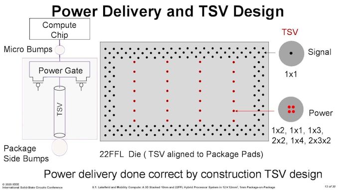
One element key to the base interposer and IO silicon is that it also has to carry power up to the compute die. With the compute die being on top to aid in the cooling configuration, it still has to get power from somewhere. Because the compute die is the more power hungry part of the design, it needs dedicated power connectivity through the package. Whereas all the data signals can move around from the compute die to the peripheral die, the power needs to go straight through. As a result, there are a number of power oriented ‘through silicon vias’ (TSVs) that have to be built into the design of the peripheral part of the processor.
Power and High Speed IO
Here’s a more complex image from a presentation earlier this year. It shows that Intel is using two types of connection from the bottom die to the top die: signal (data) connections and power connections. Intel didn’t tell us exactly how many connections are made between the two die, stating it was proprietary information, but I’m sure we will find out in due course when someone decides to put the chip in some acid and find out properly.
However, some napkin math shows 28 power TSV points, which could be in any of the configurations to the right – those combinations have a geometric mean of 3.24 pads per point listed, so with 28 points on the diagram, we’re looking at ~90 power TSVs to carry the power through the package.
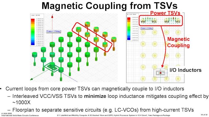
Normally passing power through a horizontal or vertical plane has the potential to cause disturbance to any signalling nearby – Intel did mention that their TSV power implementations are actually very forgiving in this instance, and the engineers ‘easily’ built sufficient space for each TSV used. The 22FLL process helped with this, but also the very low density of the process needed gave plenty of room.
From this slide we can see that the simulations on TSVs in the base die required different types of TSV to be interleaved in order to minimize different electrical effects. High current TSVs are very clearly given the widest berth in the design.
When it comes to the IO of the bottom die, users might see that PCIe 3.0 designation and baulk – here would be a prime opportunity for Intel to announce a PCIe 4.0 product, especially with a separate focused IO silicon chiplet design. However, Lakefield isn’t a processor that is going to be paired with a discrete GPU, and these PCIe lanes are meant for additional peripherals, such as a smartphone modem.
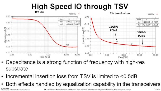
Not to be discouraged, Intel has presented that it has looked into high-speed IO through its die-to-die interconnect.
In this case, Intel battles capacitance as the higher frequency requirements of newer PCIe specifications. In this instance the signal insertion loss difference between PCIe 4.0 and PCIe 5.0 is fairly low, and well within a 0.5 dB variance. This means that this sort of connectivity might see its way into future products.
Memory
Also built into the package is the onboard memory – in this case it is DRAM, not any form of additional cache. The PoP memory on top (PoP stands for Package on Package) comes from a third party, and Intel assembles this at manufacturing before the product is sold to its partners. Intel will offer Lakefield with 8 GB and 4 GB variants, both built on some fast LPDDR4X-4266 memory.
In our conversations with Intel, the company steadfastly refuses to disclose who is producing the memory, and will only confirm it is not Intel. It would appear that the memory for Lakefield is likely a custom part specifically for Intel. We will have to wait until some of our peers take the strong acids to a Lakefield CPU in order to find out exactly who is working with Intel (or Intel could just tell us).
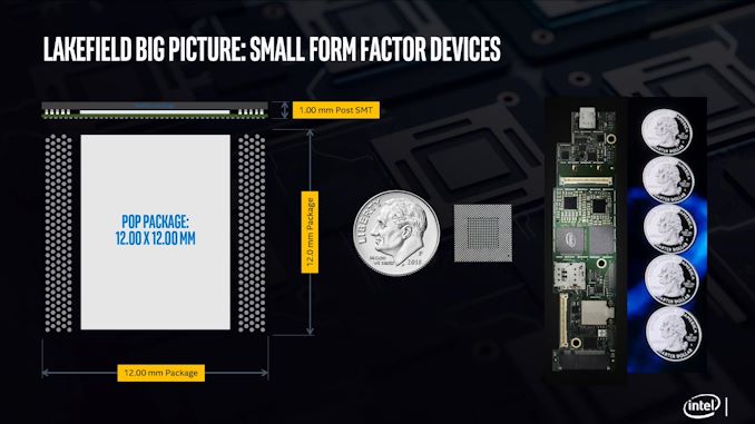
The total height, including DRAM, should be 1 mm.
As mentioned earlier in the article, Intel moving to chiplets one on top of the other exchanges the tradeoff of package size for one of cooling, especially when putting two computationally active parts of silicon together and then a big hunk of DRAM on top. Next we’ll consider some of the thermal aspects to Lakefield.
Thermal Management on Stacked Silicon
With a standard processor design, there is a single piece of silicon doing all the work and generating the heat – it’s bonded to the package (which doesn’t do any work) and then depending on the implementation, there’s some adhesive to either a cooler or a headspreader then a cooler. When moving to a stacked chiplet design, it gets a bit more complicated.
Having two bits of silicon that ‘do work’, even if one is the heavy compute die and the other is an active interposer taking care of USB and audio and things, does mean that there’s a thermal gradient between the silicon, and depending on the bonding, potential for thermal hotspots and build-up. Lakefield makes it even more complex, by having an additional DRAM package placed on top but not directly bonded.
We can take each of these issues independently. For the case of die-on-die interaction, there is a lot of research going into this area. Discussions and development about fluidic channels between two hot silicon dies have been going on for a decade or longer in academia, and Intel has mentioned it a number of times, especially when relating to a potential solution of its new die-to-die stacking technology.
They key here is hot dies, with thermal hotspots. As with a standard silicon design, ideally it is best to keep two high-powered areas separate, as it gives a number of benefits with power delivery, cooling, and signal integrity. With a stacked die, it is best to not have hotspots directly on top of each other, for similar reasons. Despite Intel using its leading edge 10+ process node for the compute die, the base die is using 22FFL, which is Intel’s low power implementation of its 14nm process. Not only that, but the base die is only dealing with IO, such as USB and PCIe 3.0, which is essentially fixed bandwidth and energy costs. What we have here is a high-powered die on top of a low powered die, and as such thermal issues between the two silicon die, especially in a low TDP device like Lakefield (7W TDP), are not an issue.
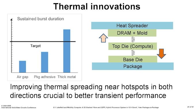
What is an issue is how the compute die gets rid of the heat. On the bottom it can do convection by being bonded to more silicon, but the top is ultimately blocked by that DRAM die. As you can see in the image above, there’s a big air gap between the two.
As part of the Lakefield design, Intel had to add in a number of design changes in order to make the thermals work. A lot of work can be done with the silicon design itself, such as matching up hotspots in the right area, using suitable thickness of metals in various layers, and rearranging the floorplan to reduce localized power density. Ultimately both increasing the thermal mass and the potential dissipation becomes high priorities.
Lakefield CPUs have a sustained power limit of 7 watts – this is defined in the specifications. Intel also has another limit, known as the turbo power limit. At Intel’s Architecture Day, the company stated that the turbo power limit was 27 watts, however in the recent product briefing, we were told is set at 9.5 W. Historically Intel will let its OEM partners (Samsung, Lenovo, Microsoft) choose its own values for these based on how well the design implements its cooling – passive vs active and heatsink mass and things like this. Intel also has another factor of turbo time, essentially a measure of how long the turbo power can be sustained for.
When we initially asked Intel for this value, they refused to tell us, stating that it is proprietary information. After I asked again after a group call on the product, I got the same answer, despite the fact that I informed the Lakefield team that Intel has historically given this information out. Later on, I found out through my European peers that in a separate briefing, they gave the value of 28 seconds, to which Intel emailed me this several hours afterwards. This value can also be set by OEMs.
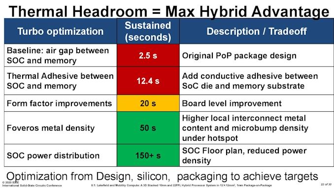
Then I subsequently found one of Intel’s ISSCC slides.
This slide shows that a basic implementation would only allow sustained power for 2.5 seconds. Adding in an adhesive between the top die and the DRAM moves up to 12.4 seconds, and then improving the system cooling goes up to 20 seconds. The rest of the improvements work below the compute die: a sizeable improvement comes from increasing the die-to-die metal density, and then an optimized power floor plan which in total gives sustained power support for 150+ seconds.
Hybrid CPUs: Sunny Cove and Tremont
Now that we’ve gone over the concept of the heterogeneous core design, it’s time to dig into each of the cores separately and some of the tradeoffs that Intel has had to do in order to get this to work.
Big Sunny Cove
As mentioned previously, the big core in Lakefield is known as Sunny Cove, and stands as the same core we currently see in Intel’s Ice Lake mobile processors today. It is officially Intel’s second 10nm-class core (the first one being the DOA Cannon Lake / Palm Cove), but the first one in mass production.
We have covered the Sunny Cove core microarchitecture in great detail, and you can read about it here:
Examining Intel's Ice Lake Processors: Taking a Bite of the Sunny Cove Microarchitecture
The quick recap is as follows.
Very similar to a Skylake design, except that:
- Better prefetchers and branch predictors
- +50% L1 Data Cache
- +100% L1 Store Bandwidth
- +100% L2 Cache w/improved L2 TLB
- +50% Micro-op Cache
- +25% uops/cycle into reorder buffer
- +57% reorder buffer size
- +25% execution ports
- AVX-512 with VNNI
The side effect of increasing the L1 Data cache size was a decrease in latency, with the L1-D moving to a 5-cycle rather than a 4-cycle. Normally that would sound like a 25% automatic speed drop, however the increased L1 size, L1 bandwidth, and L2 cache all help for an overall improvement.
Intel claimed that Sunny Cove should perform ~18% better clock-for-clock compared to a Skylake core design. In our initial review of Ice Lake, we compared the i7-1065G7 processor (Ice Lake) to the Core i9-9900K processor (Coffee Lake, a Skylake derivative), and saw a 19% increase in performance per clock, essentially matching Intel’s advertised numbers.
(However it should be noted that overall we didn’t see that much of an improvement at the overall chip and product level, because the Ice Lake ran at a lower frequency, which removed any raw clock speed gain.)
Small Tremont Atom
Arguably the Tremont core is the more interesting of the two in the Lakefield design. Lakefield will be the first consumer product built with a Tremont core inside, and as a result we have not had a chance to test it yet. But we have gone over the microarchitecture extensively in a previous article.
Intel's new Atom Microarchitecture: The Tremont Core in Lakefield
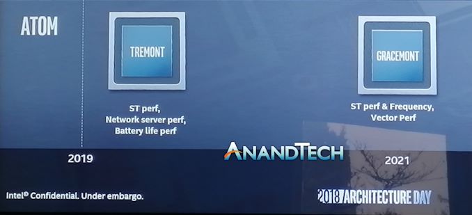
The reason why Tremont is more exciting is because updates to Intel’s Atom line of processor cores happen at a much slower pace. Traditionally Atom has been a core that focuses on the low cost part of the market, so there isn’t that much of a need to make it right at the bleeding edge as it commands lower margins for the company. It still plays a vital role, but for context, here is what year we’ve seen new Atom designs come into the market:
- 2008: Bonnell
- 2011: Saltwell
- 2013: Silvermont
- 2015: Airmont
- 2016: Goldmont
- 2017: Goldmont Plus
- 2020: Tremont
Tremont is the first new Atom microarchitecture design for three years, and technically only the third Atom design to be an out-of-order design. However, Tremont is a big jump in a lot of under-the-hood changes compared to Goldmont Plus.
- Can be in a 1-core, 2-core, or 4-core cluster
- +33% L1-Data Cache over Goldmont+, no performance penalty
- Configurable L2 cache per cluster, from 1.5 MB to 4.5 MB
- +50% L2 TLB (1024-entry, up from 512)
- New 2x3-wide decoder, rather than single 3-wide decoder
- +119% re-order buffer (208, up from 92)
- 8 execution ports, 7 reservation stations
- 3 ALUs, 2 AGUs
- Dual 128-bit AES units
- New Instructions*
What made the most noise is the new dual 3-wide decoder. On Intel’s primary Core line, we haven’t seen much change in the decoder in recent generations – it still uses a 5-wide decoder, split between 1 complex decoder and 4 simple decoders, backed with a micro-op cache. Tremont’s new dual 3-wide decoder can manage dual data streams in order to keep the buffers further down the core fed. Intel stated that for the design targets of Tremont, this was more area and power efficient than a 6-wide decoder, or having a large micro-op cache in the processor design (Atom cores have not have micro-op caches to date). Intel states that the decoder design helps shape the back-end of the core and the balance of resources.
Also worthy of note in Tremont is the L1-Data cache. Intel moved up from a 24 KiB design to a 32 KiB design, an increase of 33%. This is mostly due to using the latest manufacturing node. However, an increase in cache size is typically accompanied with an increase in latency – as we saw on Sunny Cove, we moved from a 4-cycle to a 5-cycle. However in Tremont’s case, the L1-Data cache stays at 3-cycle for an 8-way 32 KiB design. Even Skylake’s L1-D cache, at an 8-way 32 KiB design, is a 4-cycle, which means that Tremont’s L1-D is tuned to surpass even Skylake here.
The final point, Tremont’s new instructions, requires a section all on its own, specifically because none of the new instructions are supported in Lakefield.
What’s Missing in Lakefield
One of the biggest issues with a heterogeneous processor design is software. Even if we go beyond the issues that come with scheduling a workload on such a device, the problem is that most programs are designed to work on whatever microarchitecture they were written for. Generic programs are meant to work everywhere, while big publishers will write custom code for specific optimizations, such as if AVX-512 is detected, it will write AVX-512.
The hair-pulling out moment occurs when a processor has two different types of CPU core involved, and there is the potential for each of them to support different instructions or commands. Typically the scheduler makes no guarantee that software will run on any given core, so for example if you had some code written for AVX-512, it would happily run on an AVX-512 enabled core, but cause a critical fault on a core that doesn’t have AVX-512. The core won’t even know it’s an AVX-512 instruction until it comes time to decode it, and just throw an error when that happens. Not only this, but the scheduler has the right to move a thread when it needs to – if it moves a thread in the middle of an instruction stream, that can cause errors too. The processor could also move a thread to prevent thermal hotspots occurring, which will then cause a fault.
There could be a situation where the programmer can flag that their code has specific instructions. In a program with unique instructions, there’s very often a check that tries to detect support, in order to say to itself something like ‘AVX512 will work here!’. However, all modern software assumes a homogeneous processor – that all cores will support all of the same instructions.
It becomes a very chicken and egg problem, to a certain degree.
The only way out of this is that both processors in a hybrid CPU have to support the same instructions completely. This means that we end up with the worst of both worlds – only instructions supported by both can be enabled. This is the lowest common denominator of the two, and means that in Lakefield we lose support for AVX-512 on Sunny Cove, but also things like GFNI, ENCLV, and CLDEMOTE in Tremont (Tremont is actually rather progressive in its instruction support).
Knowing that Lakefield was going to have to take the lowest common denominator from the two core designs, Intel probably should physically removed the very bulky AVX-512 unit from the Sunny Cove core. Looking at the die shot, it's still there - there was some question going into the recent disclosures as to whether it would still be there, but Intel has stated on the record repeatedly that they removed it. The die shot of the compute silicon shows that not to be the case.
For x86 programmers doing instruction detection by code name or core family, this might have to change. In the smartphone world, where 4+4 processor designs are somewhat the norm, this lowest common denominator issue has essentially been universally adopted. There was some slight issue with a Samsung processor that had a non-unified cache setup, which ended up being rectified in firmware. But both sets of CPUs had to rely on lowest common denominator instructions.
How To Treat a 1+4 Hybrid CPU
At the top of the article, I explained that the reason for using two different types of processor core, one big on performance and the other big on efficiency, was that users could get the best of both worlds depending on if a workload could be run efficiently in the background, or needed the high performance for a user experience interaction. You may have caught onto the fact that I also stated that because Intel is using a 1+4 design, it actually makes more sense for multi-threaded workloads to run on the four Atom cores.
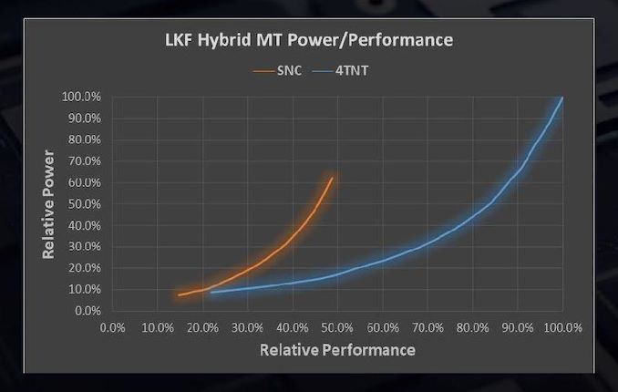
Using a similar power/performance graphs, the effect of having a 1+4 design is quite substantial. On the left is the single core power/performance graphs, but on the right is when we compare 1 Sunny Cove to all 4 Tremont cores working together.
Where the previous graph considered a 1+1 design, which is more relevant in those user experience scenarios listed above, on the right is the 1+4 design for when the user demands a heavier workload that might not be latency critical. Because there are four Atom cores, the blue line multiplies by four in both directions.
Now obviously the real world scenario is somewhere between the two, as it is possible to use only one, two, or three of the smaller cores at any given time. The CPU and the OS is expected to know this, so it can govern when workloads that can be split across multiple cores end up on either the big core or the small core.
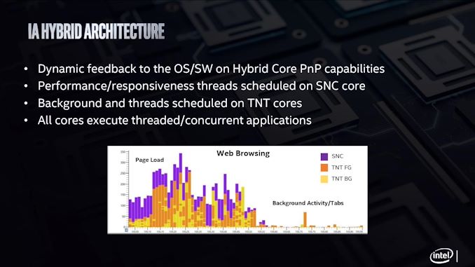
In this graph from Intel, we have three distinct modes on which threads can operate.
- ‘Sunny Cove/SNC’ is for responsiveness and user experience threads,
- ‘Tremont/TNT Foreground’, for user related tasks that require multiple threads that the user is waiting on.
- ‘Tremont/TNT Background’, for non-user related tasks run in efficiency mode
Even though the example here is web browsing, it might be best to consider something a bit beefier, like video encoding.
If we run video encoding, because it is a user related task that requires multiple threads, it will run on the four Tremont cores (TNT FG). Anything that Windows wants to do alongside that gets scheduled as TNT BG. If we then open up the start menu, because that is a responsiveness task, that gets scheduled on the SNC core.
Is 1+4 the Correct Configuration?
Intel here has implemented a 1+4 core design, however in the smartphone space, things are seen a little differently. The most popular configuration, by far, is a 4+4 design, simply because a lot of smartphone code is written to take advantage of multiple foreground or multiple background threads. There are a number of cost-down designs that reduce die area and power by going for a 2+4 implementation. Everyone seems adamant that 4 is a good number for the smaller cores, partly because they are small and cheap to add, but because Arm’s quad-core implementation is a base unit for its IP.
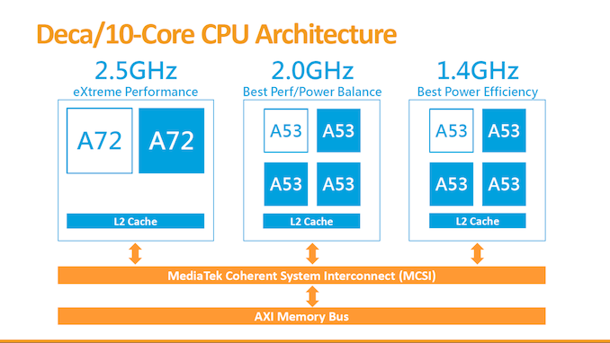
The smartphone space in recent quarters has also evolved from a two tier system of cores. In some of the more leading edge designs, we now have three types of core: a big, a middle, and a small. Because of the tendency to stay with eight core designs, we now get 1+3+4 or 2+2+4 designs, powered by complex schedulers that manage where to put the threads for the best user experience, the best battery life, or somewhere in the middle. Mediatek has been famously dabbling in 10 core designs, going for a 2+4+4 approach.
One thing missing from all of these implementations is an SoC with one big core and four small cores. Smartphone vendors don’t seem to be interested in 1+4 silicon, and yet Intel has decided on it for Lakefield. This is borne out of decisions made on both sides.
From the smartphone perspective, when hybrid designs came about, the big cores just weren’t powerful enough on their own. In order to offer something more than simply basic, at least two cores were needed, but because of how Arm architected the big and little designs, it almost became standard to look into 4+4 implementations of big and small cores. It was only until this configuration was popularized over a couple of years, and Arm big cores got more powerful, that chip designs started looking at 2+4, or 1+3+4 designs.
On Intel’s side of the fence, the biggest problem it has is the size of the Sunny Cove core. By comparison, it’s really, really big. Because the graphics core is the same as Ice Lake and reuses its design, there simply isn’t enough room within the 82 mm2 compute die to add another core. Not only that, but there is a question of power. Sunny Cove wasn’t built for sub-1W operation, even in the Tremont design. We see big smartphone silicon pulling 4-5W when all eight cores are active – there is no way, based on our understanding of Intel’s designs, that we could see four (or even two) Sunny Cove cores being in the optimal performance per watt range while being that low. Intel’s Lakefield graphics, with 64 EUs, is running at only 500 MHz – a lot lower than the Ice Lake designs. Even if Intel moved that down to a 32 EU design to make space for another Sunny Cove core, I reckon that it would eat the power budget for breakfast and then some.
Intel has made the 1+4 design to act as a 0+4 design that sometimes has access to a higher performance mode. Whereas smartphone chips are designed for all eight cores to power on for sustained periods, Lakefield is built only for 0+4 sustained workloads. And that might ultimately be its downfall. This leads onto a deep discussion about Lakefield’s performance, and what we should expect from it.
Lakefield in Terms of Laptop Size
In a traditional AMD or Intel processor designed for laptops, we experience two to eight processing cores, along with some graphics performance, and it is up to the company to build the chip with the aim of hitting the right efficiency point (15 W, or 35/45 W) to enable the best performance for a given power window. These processors also contain a lot of extra connectivity and functionality, such as a dual channel memory controller, extra PCIe lanes to support external graphics, support for USB port connectivity or an external connectivity hub, or in the case of Intel’s latest designs, support for Thunderbolt built right into the silicon without the need for an external controller. These processors typically have physical dimensions of 150 square millimeters or more, and in a notebook, when paired with the additional power delivery and controllers needed such as Wi-Fi and modems, can tend towards the board inside the system (the motherboard) totaling 15 square inches total.
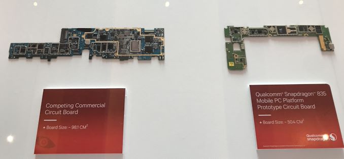
One of Qualcomm’s examples from 2018
For a Qualcomm processor designed for laptops, the silicon is a paired down to the essentials commonly associated with a smartphone. This means that modem connectivity is built into the processor, and the hardware associated with power delivery and USB are all on the scale of a smartphone. This means a motherboard designed around a Qualcomm processor will be around half the size, enabling different form factors, or more battery capacity in the same size laptop chassis.
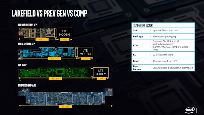
With Intel’s new Lakefield processor design, the chip is a lot smaller than previous Intel implementations. The company designed the processor from the ground up, with as much included on the CPU as to not need additional chips on the motherboard, and to fit the dimensions similar to one of Qualcomm’s processors. Above is a slide showing how Intel believes that with an LTE modem included, a Lakefield motherboard can move down to 7.7 square inches, similar to a Qualcomm design. This leaves more room for battery inside a device.
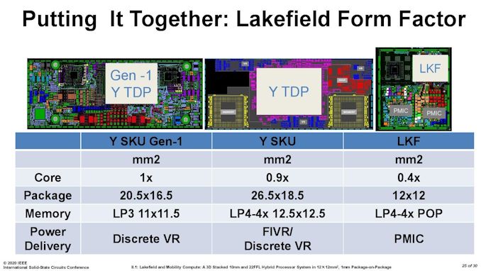
When Intel compares it against its own previous low power CPU implementations, the company quotes a 60% decrease in overall board area compared to its first generation 4.5 W processors.
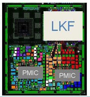
It is worth noting that for power delivery, Intel placed MIMCAPs inside the Lakefield silicon, much like a smartphone processor, and as a result it can get by on the power delivery implementation with a pair of PMICs (power management ICs). The reason why there is two is because of the two silicon dies inside – they are controlled differently for power for a number of technical reasons. If each layer within an active stacked implementation requires its own PMIC, that would presumably put an upper limit on future stacked designs – I fully expect Intel to be working on some sort of solution for this for it not to be an issue, however that wasn’t implemented in time for Lakefield.
For those that are interested, Lakefield’s PMICs are under the codenames Warren Cove and Castro Cover, and were developed in 2017-2018.
Lakefield CPUs and Devices Coming To Market
With Intel teasing Lakefield from late 2018 and stating 2020 availability, naturally we had been expecting an announcement at some point this year, and in early June the company officially announced the two processors that would be coming to the Lakefield family. Technically this is four SKUs, which I’ll get on to.
Both the parts feature ‘Core i5/i3’ branding, however they will not fall into a traditional Core generation naming. So where Skylake was 6th Gen Core, Comet Lake was 10th Gen Core, these are just ‘Intel Core Processors with Intel Hybrid Technology’. Rolls off the tongue, doesn’t it.
Both CPUs are the same silicon underneath, just with different core frequencies and GPU configurations with the Core i3 having it partly disabled.
| Intel Lakefield Processors | ||||||||
| AnandTech | Cores | Base Freq |
1C Turbo |
nT Turbo |
Gen11 IGP |
IGP Freq |
DRAM LP4 |
TDP |
| i5-L16G7 | 1+4 | 1400 | 3000 | 1800 | 64 EUs | 500 | 4267 | 7 W |
| i3-L13G4 | 1+4 | 800 | 2800 | 1300 | 48 EUs | 500 | 4267 | 7 W |
Intel confirmed that the base frequency and all-core turbo values are unified frequencies across all the cores, while the single core turbo applies to the Sunny Cove core. Support for LPDDR4X-4267 is given for both processors, and is a frequency notch above the support found in Ice Lake. The graphics is wide and slow, running at only 500 MHz, and both CPUs have a TDP of 7W. The amount of PoP memory does not affect the TDP.
However, it’s the PoP memory that will provide each one of these processors with two variants. The memory for Lakefield is being provided by a third party (Intel won’t say who, so I guess we’ll find out when we put the CPU in acid), and assembly is done by Intel. Intel will offer both processors in 4 GB and 8 GB configurations, running at a maximum memory bandwidth of 34 GB/s, indicative of dual 16-bit memory controllers. So despite the frequency of the memory being higher than Ice Lake, Ice Lake can address 4x16-bit memory controllers, giving an overall higher memory bandwidth.
Intel will debut these two SKUs in its first generation of Lakefield. Even those these CPUs are a 1+4 configuration, operating mainly in a 0+4 as mentioned on the previous pages, Intel is placing them in the premium market spaces due to the increased complexity of construction but also on the basis of the low idle power. Intel claims a 2-3 mW idle power (initially said 2 mW, then said 3 mW, then settled on 2.6 mW, depending on who you ask) while in connected standby modes. This will help any systems using them achieve long periods of sleep modes without needing to worry about casual drain.
As a result, these CPUs will find homes in premium, always-connected laptops, such as the Samsung Galaxy Book S expected in markets this month, the Lenovo ThinkPad X1 Fold, coming later this year, and in the Microsoft Surface Book Neo.
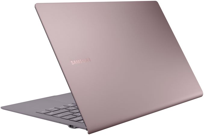
Samsung Galaxy Book S
As per our announcement piece:
First teased by Samsung late last year, the Lakefield-based version of the laptop is set to join their existing Qualcomm 8cx-based model, swapping out the Arm SoC for x86, providing a very interesting point of competition if we’re able to compare the two in the same chassis. The Intel Galaxy Book S will be the first device to ship with Lakefield, putting the new processor to the test in seeing if Intel can match the kind of all-day battery life that the existing Galaxy Book S is known for.
Taking a look at the specifications, the Intel-based version of the Galaxy Book S is a spitting image of the Qualcomm version. Samsung appears to be using the same chassis here, so the 13.3-inch laptop retains the same dimensions as the current model, as well as the same two USB-C ports. The battery capacities are identical as well at 42 Wh, and I expect that the Intel model is also using the same 1080p LCD. Curiously though, the Intel model does end up being ever so lighter than the Qualcomm model – Samsung puts the former at 950g, 10g lighter than the 960g Qualcomm model.
| Samsung Galaxy Book S Family | ||
| Galaxy Book S (Intel) | Galaxy Book S (Qualcomm) | |
| CPU | Intel Core with Hybrid Technology 1x Sunny Cove (Core) 4x Tremont (Atom) |
Qualcomm Snapdragon 8cx 4x Kryo 495 Gold @ 2.84 GHz 4x Kryo 495 Silver @ 1.8 GHz |
| GPU | Intel UHD Graphics | Adreno 680 |
| Display | 13.3 Inch, 1920×1080 Full HD Touchscreen |
|
| Memory | 8 GB LPDDR4X | |
| Storage | 256/512 GB eUFS + microSD Card Slot |
256/512 GB + microSD Card Slot |
| Networking | Wi-Fi 6 (802.11ax) BT 5.0 |
Wi-Fi 5 (802.11ac) BT 5.0 |
| Modem | Discrete LTE Cat 16 |
Integrated Qualcomm X20 LTE Cat 18 |
| Battery | 42 Wh | |
| Ports | 2 x USB-C 1 x 3.5 mm (phono/mic) |
|
| Dimensions | 305.2 x 203.2 x 11.8 mm | |
| Weight (Approx) | 950g | 960g |
| Price (USD) | N/A | Starts at $999 |
As for memory and storage, because the memory is part of the Lakefield package, Samsung is only offering a single 8GB configuration here. Unfortunately Samsung’s spec sheet doesn’t list memory frequencies, so we’ll have to wait and see what Intel has Lakefield’s memory clocked at. Meanwhile Samsung provides the storage, using 256GB or 512GB of their eUFS flash memory. To my knowledge this is the first x86 laptop to ship with eUFS, reflecting the mobile roots of the devices Intel is targeting with Lakefield. Further storage expansion is then available through a microSD card slot.
One specification that’s notably missing from Samsung’s announcement is the expected battery life of the Intel-based model, and this is perhaps going to be the most interesting aspect of Lakefield. Intel has worked very hard to get their idle power consumption down to be able to match what Qualcomm has achieved with the 8cx, with the company claiming that Lakefield draws just ~2-3mW at idle. At the same time, however, Lakefield lacks an integrated modem, and as a result Samsung is relying on an Intel Cat 16 external modem here. So in the battle of the Galaxy Books, Qualcomm will have the advantage in regards to requiring fewer chips.
As for other wireless connectivity, the new Intel model will ship with a 2x2 Wi-Fi 6 radio, giving it an edge there over the Qualcomm model with Wi-Fi 5. And both models ship with Bluetooth 5.0 support.
Rounding out the package, the Intel-based Galaxy Book S has a 720p webcam, a built-in microphone as well as Dolby Atmos-badged stereo speakers co-designed with AKG. The laptop also has a Windows Hello-compatible fingerprint reader. Price is currently unknown.
Lenovo ThinkPad X1 Fold
From our news announcement coverage:
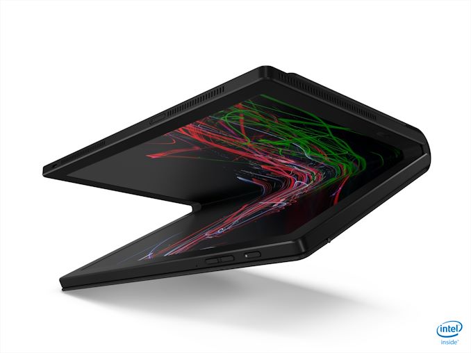
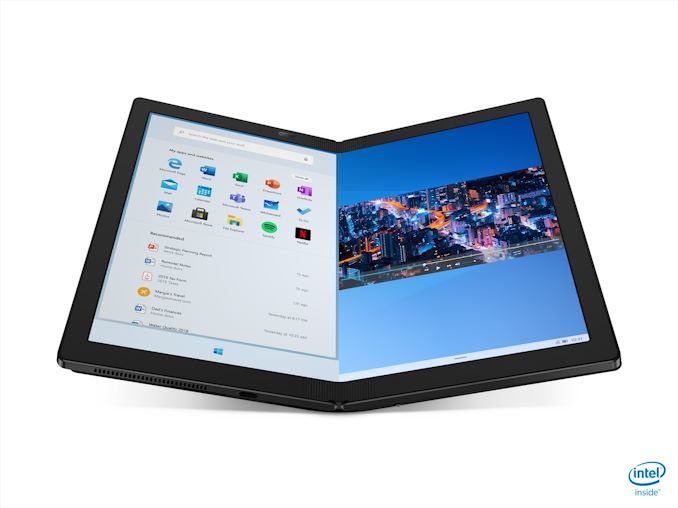
The new Fold is a true high-end Thinkpad, with a flexible 13.3-inch OLED display split across the two halves of the design, essentially becoming the size of a notepad when folded. This means that when unfolded, it offers 2x more screen real estate than a Samsung foldable smartphone. The construction of the foldable display includes metal frames and supports combined with carbon fiber plates. The hinge mechanism claims to provide friction free folding, but also allows for rigid support at a variety of angles when unfolded like a standard clamshell.
When folded, the device is just over an inch thick (27.8 mm) at its widest point, but when unfolded becomes only 7.8 mm thick, or 11.5 mm with the included cover. The reason that the folded dimension is more than 2x the unfolded is because there will be a slight ridge on the hinge where the fold is, so the display isn’t crisply folded.
Inside the unit beats the heart of a properly built laptop. We’ve got one of the first new outings for Intel’s Lakefield processor, featuring 1 big Sunny Cove core and 4 smaller Tremont Atom cores, combined with Intel’s Gen11 HD Graphics (the ones that come with Ice Lake, although it doesn’t mention frequencies or EUs). Memory is a full 8 GB of LPDDR4X-2133 with storage provided by a standard M.2 2242 NVMe drive, although Lenovo will offer variants up to 1 TB. There’s an inbuilt 5 MP camera, and the battery is a proper 50 Wh, good for 11+ hours according to Lenovo.
The exact specifications on the display is a 13.3-inch flexible OLED with a 2048x1536 resolution, with brightness up to 300 nits and color gamut support up to 95% of DCI-P3. Touch is also implemented.
For IO, the device has two USB Type-C ports (one USB 3.1, one USB 3.2), and a Displayport over Type-C port for external displays. There is also a SIM slot in order to use the onboard modem. Lenovo lists the modem as 4G/5G, although doesn’t state which modem this is – it’s likely to be Qualcomm’s X55 at this point. The device also supports 802.11ax and BT5.0.
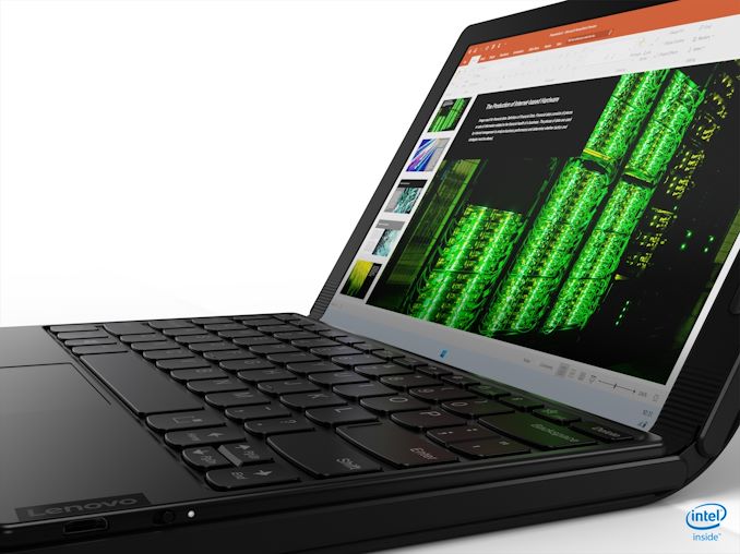
The price according to Lenovo is $2499 for the 1 TB model. All units will come with an Active Pen and an external keyboard in the box, and altogether the unit weighs 999g / 2.2 lbs (cover included). The keyboard can be off the notebook, or placed on one half of the screen:
The Lenovo ThinkPad X1 Fold looks like a crazy device that I’d love to test. Lenovo has a tentative date of ‘Mid 2020’ for the product, which will likely depend on display availability as well as Intel’s production of Lakefield processors.
Microsoft Surface Book Neo
Less is known about the Surface Book Neo. It was presented by Microsoft at an event in October 2019, featuring dual 9-inch screens and a fully rotatable hinge, and according to Microsoft’s website should be available by the end of the Holiday 2020 season.
The Neo is a true dual screen device, rather than something foldable, but will still use the external keyboard. We expect some form of pen support, and it should be running Windows 10X, a special build of Windows built for multi-screen devices like this one. However, it has been reported that Windows 10X has been delayed until next year due to the additional complexities of working from home during the pandemic as well as a focus more on single screen devices.
Performance Numbers: How To Interpret Them
On the previous page, we covered all three of the initial Lakefield designs. All three are very premium products, either offering a super light and thin clamshell with the Samsung, a foldable display with the Lenovo, or dual 9-inch displays in the case of the Microsoft device. Typically we see these sorts of devices paired with the best-in-class performance hardware, which can cost a lot depending on where it is coming from. Add in the device material cost, and we can easily go north of $999, $1499, or even higher when paired with lots of storage, or items like variable refresh displays. Make no mistake, Lakefield will end up in premium high-cost products.
This means that there will be a certain expectation of performance. Users won’t be satisfied if they get an expensive product with mid-range performance – if they’ve paid top dollar, they want it to exceed in all areas. Performance, battery life, and aesthetics all matter to the end-user when we’re dealing with things like flexible displays or new and exciting form factors on top of everything else.
Now don’t get us wrong here, Lakefield certainly fits many of the criterion of a premium product. It was specifically designed to fit into a small footprint by using novel and complex technology. By using the die-to-die bonding techniques and PoP memory, Intel has put in 174 mm2 of silicon into 12mmx12mm dimensions at only 1mm z-height. It leverages both Intel’s leading edge 10+ manufacturing node as well as Intel’s 22FFL high efficiency manufacturing node, and then optimized layout and manufacturing to ensure it has the most appropriate thermal characteristics for the design. There’s also the ultra-low idle power, supposedly measuring 2-3 mW, which has been an important characteristic in laptops that have been using smartphone processors. Offering substantial idle battery life is a key to marketing this type of product.
However, this page is about performance. Ultimately Lakefield can be compared to a number of products on the market. Numbers in brackets indicate big cores and small cores:
- Intel 7 W Lakefield (1+4) vs Qualcomm Snapdragon 7c (0+8)
- Intel 7 W Lakefield (1+4) vs Intel 6 W Goldmont+ Atom (0+4) N5030
- Intel 7 W Lakefield (1+4) vs Intel 5 W Amber Lake-Y (2+0) m3-8100Y
- Intel 7 W Lakefield (1+4) vs Intel 9 W Ice Lake-Y (2+0) 1005G1
| Comparison Table for Lakefield | |||||
| Intel i7-L16G7 |
AnandTech | Intel i3-1005G1 |
Intel m3-8100Y |
Intel N5030 |
Qualcomm SD 7c |
| Lakefield | SoC | Ice Lake-Y |
Amber Lake-Y |
Goldmont+ | Kryo |
| 1+4 | Core Config | 2+0 | 2+0 | 0+4 | 0+8 |
| 7 W | TDP | 9 W | 5 W | 6 W | ~7 W |
| 1 x SNC 4 x TNT |
CPU | 2 x SNC | 2 x SKL | 4 x GMN+ | 8 x Kryo |
| Gen 11 64 EUs 0.5 GHz |
GPU | Gen 11 32 EUs 0.9 GHz |
Gen 9 24 EUs 0.9 GHz |
Gen 9 18 EUs 750 MHz |
Adreno 618 |
| 4267 | LPDDR | 3733 | LPD3-1866 | 2400 | 4267 |
| Wi-Fi 6* | Wi-Fi | Wi-Fi 5* | - | - | Wi-Fi 6 |
| - | Modem | - | - | - | Cat15/13 |
One processor I missed out here is the Qualcomm Snapdragon 8cx, which is a 4+4 configuration that Qualcomm has specifically built for these sorts of mobile devices. The 4+4 configuration, on paper, might seem unfair to the 1+4 of Lakefield, whereas the 0+8 configuratrion of the Snapdragon 7c is more in line with what we might expect. However, the Snapdragon 7c isn’t actually inside any retail devices right now, having only been on display at Qualcomm’s own event in December.
The thing is, the Snapdragon 7c is set to be in devices competing at the $500 level against entry-level Intel Celeron devices. The 8cx is the premium chip, that ends up in the premium devices. This is where Intel will have difficulty.
On Intel’s own slides, the company performs two main comparisons.
- Benchmarks against Amber Lake-Y, the i7-8500Y in 5W mode
- Benchmarks where the i5-L16G7 runs in 1+4 and 0+4 modes
Benchmarks vs. Intel Amber Lake i7-8500Y
For the first point, Intel promotes the following against Amber Lake:
- +12% single threaded performance, measured by SPEC2006 (3.0 GHz vs 4.2 GHz)
- +70% graphics performance, 3DMark11 comparing HD615 (24 EUs, Gen 9.5 at 1.05 GHz, 2x4 GB LPDDR3-1866) vs HD (64 EUs, Gen11 at 500 MHz, 2x4 GB LPDDR4X-4267)
- +24% power efficiency, score per Watt on WebXPRT 3
- +100% AI workloads on graphics, ResNet50 batch 128 on OpenVINO, comparing
For each of these workloads, there’s something very obvious to pick at.
The first one is SPEC2006, not SPEC2017, and it’s comparing an Amber Lake core to a Sunny Cove core, which as we discussed should have +18% IPC. The frequency difference (assuming both were allowed to turbo to max) is 40% in the favor of Amber Lake, however the Lakefield has a 40% TDP advantage.
On the graphics performance, it’s a substantial mashup – Gen 9 vs Gen 11, 24 EUs vs 64 EUs, 1.05 GHz vs 500 MHz, LPDDR3-1866 vs LPDDR4X-4267. We know that Intel is going wide and slow with Lakefield, and the fact that Lakefield has an additional 40% TDP to help the graphics and CPU cores, I suspect that each chip was battling to find the right balance of power to the CPU or power to the GPU.
On the AI workload, this benchmark has been hand-picked. Intel has done an offline Resnet-50, and run the CPUs in batches. With the GPU being wide and slow, there is the question as to whether the GPU would be competitive in batch-1 type scenarios. Again, there’s also a TDP difference here, as well as a memory difference that explains the raw performance change.
Benchmarks Against Lakefield in 1+4 Mode against 0+4 Mode
For the second set of benchmarks, Intel promotes +33% higher web performance and 17% better power efficiency by adding a big core to a quartet of small cores – essentially comparing a full fat Lakefield against a quad-core Atom design.
What this means is that Lakefield, by and large, will perform the same as a quad-core Atom in almost all tasks, especially heavy tasks. Given that we haven’t had a new Atom platform since 2017, and it’s been even longer since we saw Atom notebooks in a big way, I can guarantee that a lot of users will look at Lakefield and compare it to big-core designs. Intel has also tripped over its own feet in not comparing the performance to any of Qualcomm’s designs. The cost would seem to put it square against the Snapdragon 8cx, however the core layout suggests the 7c would be a fairer fight. Putting Intel’s AI test against Qualcomm’s hardware would also make for an interesting comparison.
Another thing to note, which Intel glossed over, that most people are going to be really concerned about.
What The Big Core Is Actually For
I’ve mentioned a few times in this piece that the big Sunny Cove core is more for end-user latency driven interactions, such as tapping on the screen, typing on the keyboard. When it comes to loading a web page, this blurs the line between response and workload, depending on the browser and how it manages threads.
Now, if we take a traditional high load single threaded workload, such as say, rendering. Which core will it run on? A lot of Intel’s marketing materials, as well as considering the layout of the chip, might get a reasonable end-user to expect that it would run on the high-performance single core. However, consider two things: firstly, rendering a frame is not a latency-driven interaction. Secondly, how many processes are running in the background? Both of these elements would point to the operating system pushing the workload, despite being single threaded, onto the Tremont Atom cores.
At the time of writing, Notebookcheck is the only outlet to publish data from an early look on Samsung’s Galaxy Book S. If we take a single threaded rendering workload, like Cinebench R15, then Lakefield scores 88 points, while the Amber Lake that Intel used in its slides scores 129, a +46% performance uplift to the older Amber Lake system. What in the world is going on? It’s running on the Atom cores.
Our recommendation, for anyone wanting to test the performance of that single Sunny Cove core, is to implement an affinity mask on the software being used. If the software only knows that one core exists, then it can only run on that core. This is how we suspect that Intel achieved the single core performance gains in benchmarks like SPEC2006. However Intel has more tools at its disposal – there’s a chance that the scheduler for these systems might ignore affinity masks in order to maintain a thermal balance in the design. We must wait until we get a sample in for ourselves.
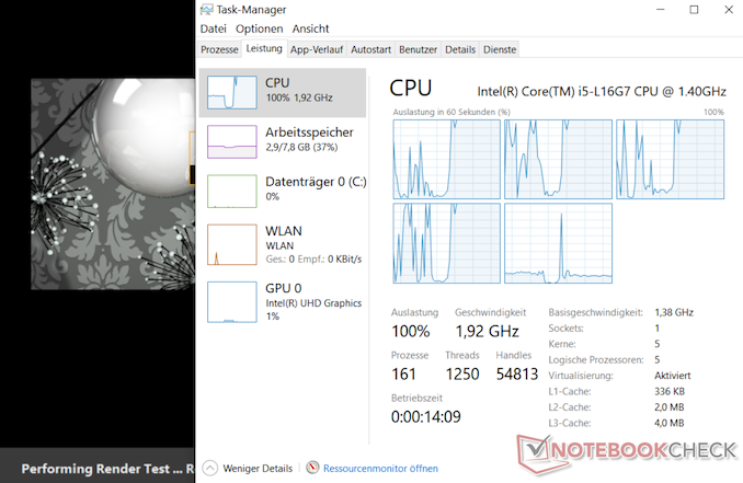
To a certain extent we see this in the Cinebench R15 multi-threaded test. With a standard 5 thread processor, if you run a standard nT test, we expect it to fill all the cores to give the best performance. In Notebookcheck’s article, we can see that the scheduler has evicted the workload from the big core. This is likely due to power/thermal hotspot reasons.
Source: Notebookcheck
In the task manager on the right, we see the first four Atom cores running at 100% while in the multi-threaded test, while the large Sunny Cove core is relatively idle. Note that the CPU is running at 1.9 GHz, and not the 2.8 GHz that Intel has promoted is the all-core turbo for this product.
But the bottom line is that in most cases, expect Lakefield to perform similar to four Atom cores, just above Goldmont Plus, and not like any of the Skylake/Ice Lake Core products and its derivatives.
The Future of Lakefield
Lakefield as a product is a lateral move for Intel. The company is taking some of its new and popular IP, and placing it into a novel form factor that has required a significant amount of R&D from a manufacturing and construction perspective. The goal of Lakefield was to meet particular customer requirements, which we understand to be around battery life, performance, and multi-screen support, and according to Intel, those goals have been met, and they will be producing future generations of Lakefield products.
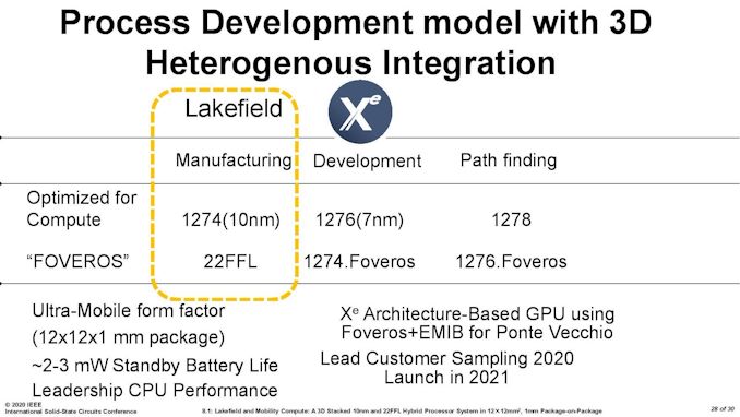
In particular, Intel has produced this slide at a couple of conferences.
This slide essentially states that Lakefield product in the yellow box has two silicon die – one optimized for compute on Intel’s P1274 process (10+ nm) and the Foveros layer (the active interposer layer) on Intel’s 22FFL process.
The next product with heterogeneous manufacturing integration will be Intel’s big Xe-HPC product, Ponte Vecchio, which will use Intel’s P1276 process (7nm) as a compute die and Intel’s P1274 (10+) process as a base interposer layer.
Beyond this, Intel looks to continue with its multi-layered products by having the compute layer on the most advanced process node, with the interposer layer one generation behind, on a ‘Foveros’ optimized variant.
So the first generation Lakefield is essentially a product that combines P1274 and 22FFL, and a future product is likely to be built on P1276 on the compute layer and P1274 for the interposer layer. Keeping this sort of cadence makes a lot of sense. However, Intel is going to have to learn from Lakefield in a number of ways, especially as we look at ways in which the heterogeneous layering concept can expand. I’ve split this into several areas that I feel is critical to where layered processors can really make a difference.
Growing a Stacked Die to Higher TDP and Core Count
I’ve combined these two points because they essentially go together. Implementing two simple silicon die together in a small form factor product, while is interesting on the power side of the equation, doesn’t probe the question of scaling the product up. It’s easy enough to scale the product out by adding in some form of connectivity to the stack and then connecting them together (which is what’s happening in Ponte Vecchio), but at some point the stack has to move to a higher level of power consumption if it wants to move upwards in power.
This means that thermals become a bigger issue if it wasn’t already. If we take the current Lakefield design, with one compute die over an active interposer, with the right routing then moving to a physically larger floorplan and a higher power shouldn’t be too much of an issue – if anything, making the base die larger should help spread a lot of that IO about, making the interposer a functionally less active interposer. Or Intel will implement the next generation of its die-to-die stacking technology, where the top dies can be larger than the base dies, in a cantilevered fashion.
The bigger deal with the thermals is going to be on the top, with the stacked PoP memory. We go more into the memory communications aspect in a bit, but ideally that memory needs to be on the side so the compute die can have access to a proper heatspreader. The only reason it is stacked in Lakefield is because of the size constraints and attempting to get everything into that small form factor. For anything larger, there needs to be a memory controller that looks outside the chip, which is kind of what we’re expecting from Ponte Vecchio with HBM. A desktop-class product would likely be in the middle.
Growing a Stacked Die to More Stacks
The other angle for a stacked silicon product is to put more stacks in place. This again brings about the question on cooling between the stacks, depending on what is actually there. Lakefield is only two stacks right now, with one high-powered stack and one low-powered stack. Intel would have to prove that it could manage multiple high-powered stacks in order to expand compute in the vertical dimension, but that brings about its own problems.
To start, with Lakefield, the main power to the top compute die is provided with TSVs going through the active interposer layer. For each compute die in a multi-die stack, there would have to be TSVs for each one in order to provide individual power. Unless the active interposer also acted as a PMIC, this could become difficult depending on what other TSVs or data paths need to be put in place between the layers.
Note, when we spoke with Intel’s Ramune Nagisetty at IEDM last year, when asked if Intel would ever discuss if a stacked product would use ‘dummy’ layers to help in cooling, we were told that this would unlikely be mentioned, focusing only on the layers that actually do any work. But ultimately there could be cause for dummy layers to aid in cooling, such that they can provide mass and distance between thermal hotspots between compute dies involved. As the number of layers increases, however, something like Lakefield would have to move the PoP memory off the top, as already mentioned.
Memory Communications
One element to the Lakefield design we haven’t really covered here is how the memory communicates. In the current Lakefield design, the compute cores and the memory controllers are located on the compute die. In order for a portion of main memory to be read into the compute die, the communication has to travel down through the active interposer, go into the package, and then loop back up to the stacked memory.
In the following diagram, on the left, we have (1) going from Compute Die to DRAM, and (2) DRAM back to Compute Die.
This path is a lot longer than simply going from the compute die straight up into the memory, which would be theoretical on the right hand side if the two were bonded and had appropriate pathways.
If a future Lakefield product wants to continue down the memory-on-top route, one optimization could be to bond that top memory die in a Foveros-like fashion. One could argue that it means Intel would have to bond the memory on at the manufacturing stage, but this already happens with the current generation of Lakefield designs. The only downside would be getting the bonding pads on the top of the compute die and the bottom of the memory die to line up, and then manage the communications from there. The power for the memory would have to also come through on TSVs.
But if we’re bonding the memory into the stack, then technically it could go at any layer – there are likely benefits to keeping the compute die/dies on top. This could lead to multiple layers of memory as needed.
Power Management
With the current Lakefield design, both the compute die and the active interposer die have their own power management IC (PMICs) in order to help deliver power. Based on Intel’s own diagrams, these PMIC designs take up more physical PCB space than Lakefield itself.
At some level, Intel is going to have to figure out to create a unified PMIC solution to cover every layer on the product. It likely reduces board space and would make things a lot simpler, as it does with laptops that can manage power to the CPU and GPU on the same die with an onboard power controller. A PMIC that can scale with layer counts is obviously going to be a plus.
Cooling
Through all of this, as I’ve mentioned several times, cooling is going to be a major concern. There’s no easy way around the physics of dissipating 5-10 W in such a small space, or over 100 W if the product scales up into something in a form factor that has a wider appeal. Previously in the article I mentioned that we had discussed this with Intel, and how areas such as microfluidic channels have obviously had some research put into, but nothing to the point where it could be done commercially and at scale. It’s a paradigm worth solving, because the benefits would be tremendous.
Beyond Windows and Enabling 5G
One thing to note is that Intel's Lakefield is only planned with Windows 10 support right now. Linux is currently not in the plan for this product, but it would have to be if Intel wants wider adoption of the technology.
Not only this, but as most people are comparing these devices to Qualcomm's hardware, appropriate 5G support will need to be applied - the current generation Lakefield is not part of Intel and Mediatek's collaboration on 5G, which only applies to Tiger Lake and beyond. Lakefield customers will have to rely on 4G as an optional extra, or 5G through an external modem.
The Future Of Lakefield
Even if this first generation version of Lakefield gets slammed pretty hard in performance-focused benchmark reviews for being slower than a dual-core Whiskey Lake, Lakefield marks some very big steps for Intel. Hybrid CPU designs, and stacked die-to-die connectivity, are going to feature in Intel’s future roadmaps – at what points will depend on how much Intel is willing to experiment but also how well Intel can execute. There have been discussions on Intel perhaps looking at an 8+8 hybrid CPU design in the future, although nothing we can substantiate, but we do know that Ponte Vecchio with stacked die is coming in late 2021.
One of the key ingredients in all of this is going to be at what points Intel’s technology portfolio is going to intersect its product portfolio. Some of these technologies might find their way better suited to aspects such as 5G networking, or automotive, rather than something we can consume on the desktop. As far as Lakefield goes, this first generation is going to be a rough challenge for Intel – they are pitching a low performance product in a high-cost segment based on technology (and to a certain extent, battery life). Die-to-die stacking will get easier to do as scale ramps, and hopefully new process node technologies will drive the power efficiency of those big cores lower to enable 2+4 or bigger designs when in a stacked form factor.
We eagerly await a chance to test 1st Gen Lakefield, but we’re also keeping an eye on what might be in the second and third generations.

