SK Hynix: We're Planning for DDR5-8400 at 1.1 Volts
by Gavin Bonshor on April 3, 2020 1:15 PM EST
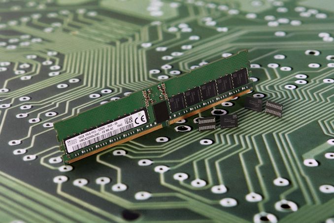
Back in November last year, we reported that SK Hynix had developed and deployed its first DDR5 DRAM. Fast forward to the present, and we also know SK Hynix has recently been working on its DDR5-6400 DRAM, but today the company has showcased that it has plans to offer up to DDR5-8400, with on-die ECC, and an operating voltage of just 1.1 Volts.
WIth CPU core counts rising with the fierce battle ongoing between Intel and AMD in the desktop, professional, and now mobile markets, the demand to increase throughput performance is high on the agenda. Memory bandwidth by comparison has not been increasing as much, and at some level the beast needs to be fed. Announcing more technical details on its official website, SK Hynix has been working diligently on perfecting its DDR5 chips with capacity for up to 64 Gb per chip.
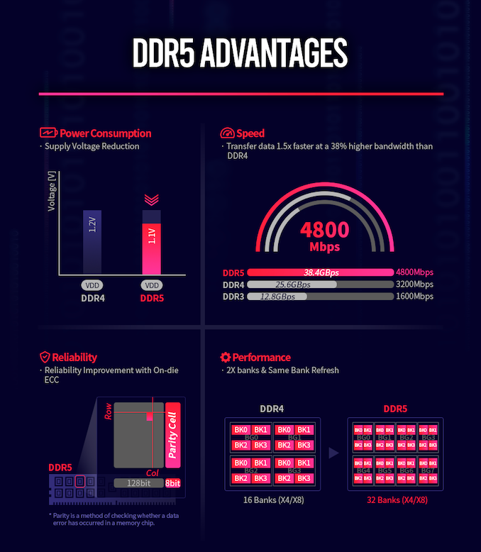
SK Hynix had previously been working on its DDR5-6400 DRAM, which has 16 Gb which is formed of 32 banks, with 8 bank groups, with double the available bandwidth and access potential when compared with DDR4-3200 memory. For reference, DDR4 uses 16 banks with 4 bank groups. The key solution to improve access throughout is the burst length, which has been doubled to 16 when compared with 8 on DDR4. Another element to consider is DDR4 can't by proxy run operations while it's refreshing. DDR5 is using SBRF (same bank refresh function) which allows the system the ability to use other banks while one is refreshing, which in theory improves memory access availability.
As we've already mentioned, SK Hynix already has DDR5-6400 in its sights which are built upon its second-generation 10nm class fabrication node. SK Hynix has now listed that it plans to develop up to DDR5-8400. Similar in methodology to its DDR5-6400 DRAM, DDR5-8400 requires much more forethought and application. What's interesting about SK Hynix's DDR5-8400 is the jump in memory banks, with DDR5-8400 using 32 banks, with 8 bank groups.
Not just content at increasing overall memory bandwidth and access performance over DDR4, the new DDR5 will run with an operating voltage of 1.1 V. This marks a 9% reduction versus DDR4's operating voltage which is designed to make DDR5 more power-efficient, with SK Hynix reporting that it aims to reduce power consumption per bandwidth by over 20% over DDR4.
To improve performance and increase reliability in server scenarios, DDR5-8400 will use on-die ECC (Error Correction) and ECS (Error Check and Scrub) which is a milestone in the production of DDR5. This is expected to reduce overall costs, with ECS recording any defects present and sends the error count to the host. This is designed to improve transparency with the aim of providing enhanced reliability and serviceability within a server system. Also integrated into the design of the DDR5-8400 DRAM is Decision Feedback Equalization (DFE), which is designed to eliminate reflective noise when running at high speeds. SK Hynix notes that this increases the speed per pin by a large amount.
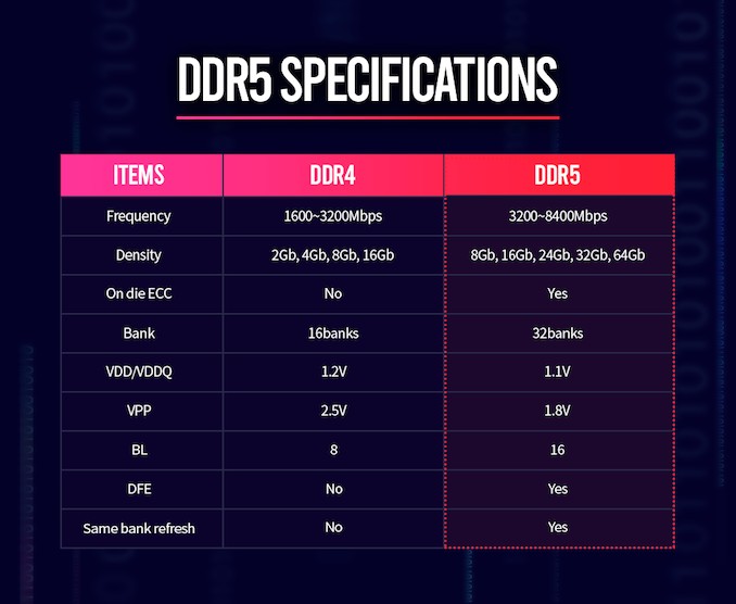
In the above image from specification comparison between DDR4 and DDR5 from SK Hynix, one interesting thing to note is that it mentions DRAM chips with density up to 64 gigabit. We already know that the chip size of DDR5 is 65.22mm², with a data rate of 6.4 Gbps per pin, and uses its 1y-nm 4-metal DRAM manufacturing process. It is worth pointing out that the DDR5-5200 RDIMM we reported on back in November 18, uses 16 Gb DRAM chips, with further scope to 32 Gb reported. SK Hynix aims to double this to 64 Gb chips which do double the density, at lower power with 1.1 volts.
Head of DRAM Product Planning at SK Hynix, Sungsoo Ryu stated that:
"In the 4th Industrial Revolution, which is represented by 5G, autonomous vehicle, AI, augmented reality (AR), virtual reality (VR), big data, and other applications, DDR5 DRAM can be utilized for next-gen high-performance computing and AI-based data analysis".
SK Hynix if still on schedule with the current Coronavirus COVID-19 pandemic, looks set to enter mass production of DDR5 later this year.
Related Reading
Source: SK Hynix


84 Comments
View All Comments
shabby - Friday, April 3, 2020 - link
1.1v at what amps?mode_13h - Friday, April 3, 2020 - link
All of them.CaedenV - Friday, April 3, 2020 - link
1.1V but with absolutely 0 resistanceshabby - Friday, April 3, 2020 - link
I'm serious, what's the point of touting lower voltage all the time. Intel chips way back when used to run at 3.3volts now they run at 1 volt yet use up 100watts+.willis936 - Friday, April 3, 2020 - link
https://en.wikipedia.org/wiki/Dynamic_frequency_sc...dullard - Friday, April 3, 2020 - link
DDR4 memory has roughly a 0.5 ohm resistance (varies with make, model, speed, etc). Power = Voltage ^2 / resistance. So at 1.2 V it will use roughly (1.2 V)^2/(0.5 ohm) = 2.88 W power.The same memory at 1.1 V would then use (1.1 V)^2/(0.5 ohm) = 2.42 W power. At 1.2 V, it uses 19% more power than at 1.1 V. Of course, that all depends on the load on the memory. It only uses full power when in use.
Newer CPUs run on lower voltage which vastly helps power. But, they are also getting larger in a parallel fashion. Overall resistance drops when in more resistors are in parallel. Thus, a many core chip could have a very low resistance and use even more power than a low core count chip with a higher voltage.
But, since power goes with voltage squared, the most important thing for power reduction is a voltage reduction.
InTheMidstOfTheInBeforeCrowd - Saturday, April 4, 2020 - link
Uh... your simplification with regard to resistance would only hold water if the CPUs would be clocked with DC (or a rather low-frequency clock). But they aren't. The transistors in the circuits switch with a frequency of several hundred or thousand MHz. With regard to power and power losses, frequency-dependent cost such as gate-charge costs supremely dominate over any resistive costs with such high frequencies in mind.So, no. Your assumption that more cores "in parallel" is like wiring resistors in parallel is wrong, unless you would only consider the silly scenario of clocking the CPU/switching the CPU transistors at a few (kilo) Hertz. The more cores, the more transistors. The more transistors, the more gates with their associated gate losses. The higher the switching frequency of the transistors, the higher the gate losses. Etc, etc...
Brane2 - Saturday, April 4, 2020 - link
Dynamic power consumptions scales roughly the same as would pure resistive losses.linuxgeex - Tuesday, April 7, 2020 - link
You mean dynamic power consumption has to live within the limits granted by Ohm's Law. :-) There's definitely moments when dynamic load can temporarily appear to ignore Ohm's Law... ie exhibiting imaginary impedance while a magnetic field collapses. But an AC circuit can never draw more current than a DC one with the same voltage and resistance.linuxgeex - Tuesday, April 7, 2020 - link
Yes, with AC circuits (anything with signalling is AC) the formula is Voltage*Charge*Frequency, not Voltage*Voltage/ResistanceResistance does still become a limiting factor in AC circuits though. If the power supply to the DRAM modules has a 1/2 Ohm resistance and a supply voltage of 1.1V then the maximum possible wattage that can be drawn from it is still V*V/R = 2.42W. For those of you not familiar with basic electronics concepts, google 'impedance matching'.