The AMD Radeon R9 Fury X Review: Aiming For the Top
by Ryan Smith on July 2, 2015 11:15 AM ESTThe Fiji GPU: Go Big or Go Home
Now that we’ve had a chance to take a look at the architecture backing Fiji, let’s talk about the Fiji GPU itself.
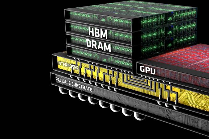
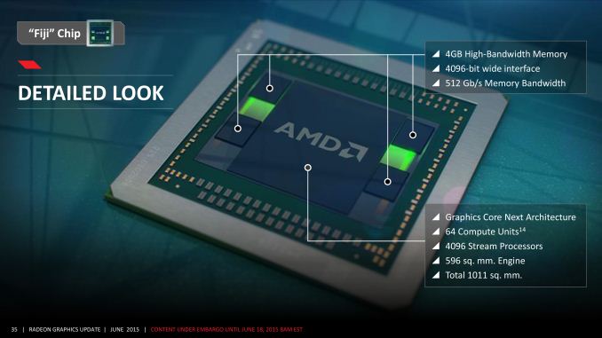
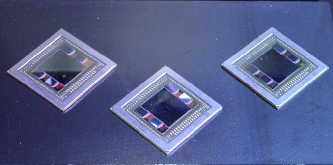
Fiji’s inclusion of High Bandwidth Memory (HBM) technology complicates the picture somewhat when talking about GPUs. Whereas past GPUs were defined by the GPU die itself and then the organic substrate package it sits on, the inclusion of HBM requires a third layer, the silicon interposer. The job of the interposer is to sit between the package and the GPU, serving as the layer that connects the on-package HBM memory stacks with the GPU. Essentially a very large chip without any expensive logic on it, the silicon interposer allows for finer, denser signal routing than organic packaging is capable of, making the ultra-wide 4096-bit HBM bus viable for the first time.
We’ll get to HBM in detail in a bit, but it’s important to call out the impact of HBM and the interposer early, since they have a distinct impact on how Fiji was designed and what its capabilities are.
As for Fiji itself, Fiji is unlike any GPU built before by AMD, and not only due to the use of HBM. More than anything else, it’s simply huge, 596mm2 to be precise. As we mentioned in our introduction, AMD has traditionally shied away from big chips, even after the “small die” era ended, and for good reason. Big chips are expensive to develop, expensive to produce, take longer to develop, and yield worse than small chips (this being especially the case early-on for 40nm). Altogether they’re riskier than smaller chips, and while there are times where they are necessary, AMD has never reached this point until now.
The end result is that for the first time since the unified shader era began, AMD has gone toe-to-toe with NVIDIA on die size. Fiji’s 596mm2 die size is just 5mm2 (<1%) smaller than NVIDIA’s GM200, and more notably still hits TSMC’s 28nm reticle limit. TSMC can’t build chips any bigger than this; Fiji is as big a chip as AMD can order.
| AMD Big GPUs | ||||
| Die Size | Native FP64 Rate | |||
| Fiji (GCN 1.2) | 596mm2 | 1/16 | ||
| Hawaii (GCN 1.1) | 438mm2 | 1/2 | ||
| Tahiti (GCN 1.0) | 352mm2 | 1/4 | ||
| Cayman (VLIW4) | 389mm2 | 1/4 | ||
| Cypress (VLIW5) | 334mm2 | 1/5 | ||
| RV790 (VLIW5) | 282mm2 | N/A | ||
Looking at Fiji relative to AMD’s other big GPUs, it becomes very clear very quickly just how significant this change is for AMD. When Hawaii was released in 2013 at 438mm2, it was already AMD’s biggest GPU ever for its time. And yet Fiji dwarfs it, coming in at 158mm2 (36%) larger. The fact that Fiji comes at the latter-half of the 28nm process’s life time means that such a large GPU is not nearly as risky now as it would have been in 2011/2012 (NVIDIA surely took some licks internally on GK110), but still, nothing else we can show you today can really sell the significance of Fiji to AMD as much as the die size can.
And the fun doesn’t stop there. Along with producing the biggest die they could, AMD has also more or less gone the direction of NVIDIA and Maxwell in the case of Fiji, building what is unambiguously the most gaming/FP32-centric GPU the company could build. With GCN supporting power-of-two FP64 rates between 1/2 and 1/16, AMD has gone for the bare minimum in FP64 performance that their architecture allows, leading to a 1/16 FP64 rate on Fiji. This is a significant departure from Hawaii, which implemented native support for ½ rate, and on consumer parts offered a handicapped 1/8 rate. Fiji will not be a FP64 powerhouse – its 4GB of VRAM is already perhaps too large of a handicap for the HPC market – so instead we get AMD’s best FP32 GPU going against NVIDIA’s best FP32 GPU.
AMD’s final ace up their sleeve on die size is HBM. Along with HBM’s bandwidth and power benefits, HBM is also much simpler to implement, requiring less GPU space for PHYs than GDDR5 does. This is in part due to the fact that HBM stacks have their own logic layer, distributing some of the logic on to each stack, and furthermore a benefit of the fact that the signaling logic that remains doesn’t have to be nearly as complex since the frequencies are so much lower. 4096-bits of HBM PHYs still takes up a fair bit of space – though AMD won’t tell us how much – but it’s notably lower than the amount of space AMD was losing to Hawaii’s GDDR5 memory controllers.
The end result is that not only has AMD built their biggest GPU ever, but they have done virtually everything they can to maximize the amount of die space they get to allocate to FP32 and rendering resources. Simply put, AMD has never reached so high and aimed for parity with NVIDIA in this manner.
Ultimately this puts Fiji’s transistor count at 8.9 billion transistors, even more than the 8 billion transistors found in NVIDIA’s GM200, and, as expected, significantly more than Hawaii’s 6.2 billion. Interestingly enough, on a relative basis this is almost exactly the same increase we saw with Hawaii; Fiji packs in 43.5% more transistors than Hawaii, and Hawaii packed in 43.9% more transistors than Tahiti. So going by transistors alone, Fiji is very much to Hawaii what Hawaii was to Tahiti.
Finally, as large as the Fiji GPU is, the silicon interposer it sits on is even larger. The interposer measures 1011mm2, nearly twice the size of Fiji. Since Fiji and its HBM stacks need to fit on top of it, the interposer must be very large to do its job, and in the process it pushes its own limits. The actual interposer die is believed to exceed the reticle limit of the 65nm process AMD is using to have it built, and as a result the interposer is carefully constructed so that only the areas that need connectivity receive metal layers. This allows AMD to put down such a large interposer without actually needing a fab capable of reaching such a large reticle limit.
What’s interesting from a design perspective is that the interposer and everything on it is essentially the heart and soul of the GPU. There is plenty of power regulation circuitry on the organic package and even more on the board itself, but within the 1011mm2 floorplan of the interposer, all of Fiji’s logic and memory is located. By mobile standards it’s very nearly an SoC in and of itself; it needs little more than external power and I/O to operate.


458 Comments
View All Comments
Agent Smith - Thursday, July 2, 2015 - link
Cheers Ryan!der - Thursday, July 2, 2015 - link
ANANDTECH KILLED THIS REVIEW!RealBeast - Thursday, July 2, 2015 - link
@der, go take your medicine and get back into your padded cell.Great review Ryan, a bit sad that AMD cannot get ahead on anything these days.
They really need to pull out a rabbit to give NVIDIA and/or Intel something to chase for a change.
They must realize that their survival is at stake.
versesuvius - Thursday, July 2, 2015 - link
Nano is the card to wait for. It will sell millions and millions and millions. And AMD is a fool to offer it for anything over $300. Despite the 4 GB ram limitation, it will run every game currently on the market and in the next 4 years fine on average to high systems which is the absolute, dictatorial majority of systems kids all over the world play on. The Enthuuuuusiasts can philosophize all they can, but it does not change anything. The size and power requirements of Nano makes is the card of choice from 1 to Entusiast - 1 range of computer users from home to academia to industry. Well done AMD.IlllI - Thursday, July 2, 2015 - link
great article, I've got a few questions.what is the difference between edram and hbm?
do you think we'll ever see hbm on a cpu?
do you think better amd drivers will close the performance gap in lower resolutions?
do you think nvidia pays companies to optimize for their gpus and put less focus on amd gpus? especially in 'the way it is meant to be played' sponsored games?
Kevin G - Thursday, July 2, 2015 - link
eDRAM uses a single die or integrated on-die with logic. HBM is composed of several DRAM dies stacked on top of each other.eDRAM tends to be connected via a proprietary link making each implementation unique where as HBM has a JEDEC standard interface.
HBM on a CPU is only a matter of time. Next year HBM2 arrives and will bring capacities that a complete consumer system can utilize.
Fjij seemingly does have some driver issues due to some weird frame time spikes. Fixing these will resolute in a smooth experience but likely won't increase the raw FPS could by much.
With DX12 and Vulkan coming, I'd expect titles just going into development will focus on those new APIs than any vendor specific technology. This does mean that the importance of drivers will only increase.
ajlueke - Thursday, July 2, 2015 - link
"HBM on a CPU is only a matter of time." That is actually one of the more interesting and exciting things coming out of the Fiji launch. The effect of slower system memory on AMD APUs has been pretty well documented. It will be interesting to see if we get socket AM4 motherboards with built in HBM2 memory for APUs to use as opposed to using system ram at all. It's also exciting to see that Nvidia is adopting this memory the next go around and who knows how small and powerful they can get their own GPUs to be. Definitely a great time for the industry!Since the Fury X is reasonably close to the 980 Ti, I would love to pick one up. AMD put a lot of the legwork in developing HBM, and without the Fury X, Nvidia likely wouldn't have even created the $649 variant that essentially obsoleted the Titan X. For those reasons feel like they deserve my money. And also I do want to play around with custom BIOS on this card a bit.
Now...if only there were any available. Newegg? Tiger? Amazon? Anyone? If they can't keep the supply chains full, impatience might drive me to team green after all.
silverblue - Friday, July 3, 2015 - link
Nah, just HBM for graphics memory. As HSA APUs shouldn't require the memory to be in two places at the same time, this will alleviate the latency of copying data from system memory to graphics memory. What's more, they don't really need more than 2GB for an APU.I'm not sure, however, that such bandwidth will make a massive difference. The difference in performance between 2133MHz and 2400MHz DDR3 is far smaller than that between 1866 and 2133 in general. You'd need to beef up the APU to take advantage of the bandwidth, which in turn makes for a larger chip. 2GB would have 250GB/s+ bandwidth with HBM1 at 500MHz, nearly ten times what is currently available, and it would seem a huge waste without more ROPs at the very least. At 14nm, sure, but not until then.
silverblue - Friday, July 3, 2015 - link
Fixing the peaks and troughs would improve the average frame rates a little, I imagine, but not by a large amount.Drivers are a sore point especially considering the CPU load in GRID Autosport for the Fury X. Could they not just contract some of this out? VCE was unsupported for a while, TrueAudio looks to be going to same way, and if NVIDIA's drivers are less demanding than AMD's, surely there must be something that can be done to improve the situation?
ajlueke - Thursday, July 2, 2015 - link
"do you think nvidia pays companies to optimize for their gpus and put less focus on amd gpus? especially in 'the way it is meant to be played' sponsored games?"I have noticed quite a few people spitting fire about this all over the interwebs these days. The state of PC ports in general is likely more to blame than anything NVidia is doing to sabotage AMD.
To differentiate the PC versions from their console counterparts and get people like us to buy $600 video cards the PC versions need some visual upgrades. That can included anything from high res textures to Physics and particle and hair effects. That is what NVidias Gameworks is all about. Most of the rumors surrounding NVidia deliberately deoptimizing a game at the expense of AMD revolve around Hairworks and Witcher 3. Hairworks is based off tessellation, which NVidia GPUs excel at compared to their AMD counterparts. Now why didn't NVidia just employ TressFX, a similar hair rendering technology used in tomb raider that performed well on both cards?
TressFX is actually a DirectCompute based technology co-developed by AMD. NVidia scaled back much of the DirectCompute functionality in their Maxwell 2 GPUs to avoid cannibalizing their own workstation GPU business. Workstation GPU margins tend to be extremely high, as businesses can afford to shell out more dough for hardware. The Titan Black was such a DirectCompute beast, that many workstation users purchased it over much higher priced workstation cards. The Titan X and GTX 980 are now far less attractive options for workstations, but unable to perform as well using TressFX. The solution is to develop a technology using what your GPU does do well "tessellation", and get developers to use it. The decision was likely made purely for business reasons and only hurt AMD as tessellation was a weak point for their cards, although less so for the R9 Fury X.
The real problem here is likely shoddy PC ports in general. Big studio titles generally are developed for console first, and ported to PC later. In the previous console generation that meant having a group develop a title for the PowerPC based Xbox 360, the Cell based PS3, and then finally porting to x86 based PC systems often after the console titles had already launched.
With the shift to the new generation of consoles, both the Xbox One and Sony PS4 are AMD x86 based. Meaning it should be extremely easy to port these games to similarly x86 based PCs. However, Mortal Kombat X, and Batman Arkham Knight are two titles that recently had horrendous PC launches. In both cases the port was farmed out to a studio other than the primary studio working on the console version. The interesting part is that MKX was not a Gameworks title, while Arkham Knight was offered for free with 980 Ti video cards. I highly doubt NVidia would add Gameworks purely to screw over AMD when the result was a major title they promoted with their flagship card doesn't even work. It is actually a huge embarrassment. Both more NVidia, but more so for the studio handling the PC port. The new console era was supposed to be a golden age for PC ports, but instead it seems like and excuse for studios to farm the work out and devote even less time to the PC platform. A trend I hope doesn't continue.