Apple's M1 Pro, M1 Max SoCs Investigated: New Performance and Efficiency Heights
by Andrei Frumusanu on October 25, 2021 9:00 AM EST- Posted in
- Laptops
- Apple
- MacBook
- Apple M1 Pro
- Apple M1 Max
Last week, Apple had unveiled their new generation MacBook Pro laptop series, a new range of flagship devices that bring with them significant updates to the company’s professional and power-user oriented user-base. The new devices particularly differentiate themselves in that they’re now powered by two new additional entries in Apple’s own silicon line-up, the M1 Pro and the M1 Max. We’ve covered the initial reveal in last week’s overview article of the two new chips, and today we’re getting the first glimpses of the performance we’re expected to see off the new silicon.
The M1 Pro: 10-core CPU, 16-core GPU, 33.7bn Transistors
Starting off with the M1 Pro, the smaller sibling of the two, the design appears to be a new implementation of the first generation M1 chip, but this time designed from the ground up to scale up larger and to more performance. The M1 Pro in our view is the more interesting of the two designs, as it offers mostly everything that power users will deem generationally important in terms of upgrades.
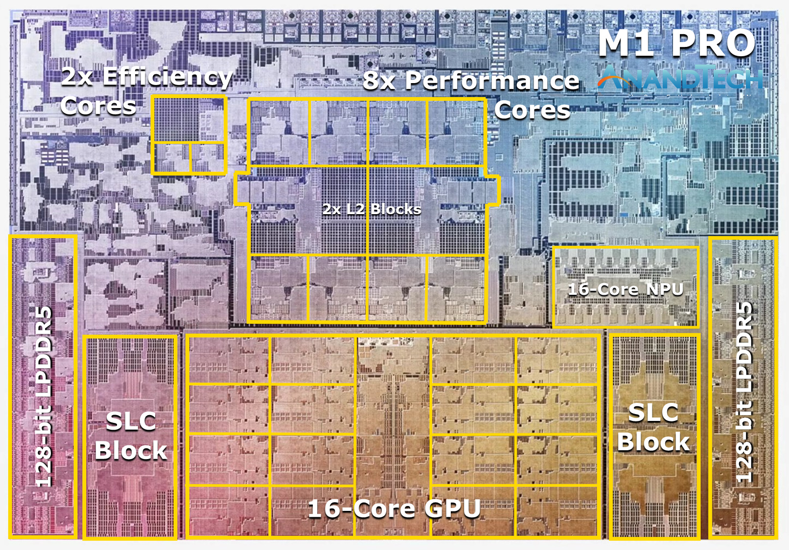
At the heart of the SoC we find a new 10-core CPU setup, in a 8+2 configuration, with there being 8 performance Firestorm cores and 2 efficiency Icestorm cores. We had indicated in our initial coverage that it appears that Apple’s new M1 Pro and Max chips is using a similar, if not the same generation CPU IP as on the M1, rather than updating things to the newer generation cores that are being used in the A15. We seemingly can confirm this, as we’re seeing no apparent changes in the cores compared to what we’ve discovered on the M1 chips.
The CPU cores clock up to 3228MHz peak, however vary in frequency depending on how many cores are active within a cluster, clocking down to 3132 at 2, and 3036 MHz at 3 and 4 cores active. I say “per cluster”, because the 8 performance cores in the M1 Pro and M1 Max are indeed consisting of two 4-core clusters, both with their own 12MB L2 caches, and each being able to clock their CPUs independently from each other, so it’s actually possible to have four active cores in one cluster at 3036MHz and one active core in the other cluster running at 3.23GHz.
The two E-cores in the system clock at up to 2064MHz, and as opposed to the M1, there’s only two of them this time around, however, Apple still gives them their full 4MB of L2 cache, same as on the M1 and A-derivative chips.
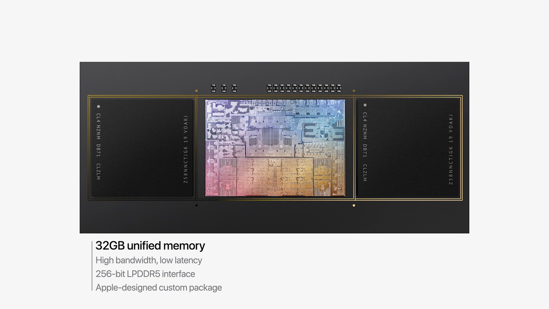
One large feature of both chips is their much-increased memory bandwidth and interfaces – the M1 Pro features 256-bit LPDDR5 memory at 6400MT/s speeds, corresponding to 204GB/s bandwidth. This is significantly higher than the M1 at 68GB/s, and also generally higher than competitor laptop platforms which still rely on 128-bit interfaces.
We’ve been able to identify the “SLC”, or system level cache as we call it, to be falling in at 24MB for the M1 Pro, and 48MB on the M1 Max, a bit smaller than what we initially speculated, but makes sense given the SRAM die area – representing a 50% increase over the per-block SLC on the M1.
The M1 Max: A 32-Core GPU Monstrosity at 57bn Transistors
Above the M1 Pro we have Apple’s second new M1 chip, the M1 Max. The M1 Max is essentially identical to the M1 Pro in terms of architecture and in many of its functional blocks – but what sets the Max apart is that Apple has equipped it with much larger GPU and media encode/decode complexes. Overall, Apple has doubled the number of GPU cores and media blocks, giving the M1 Max virtually twice the GPU and media performance.
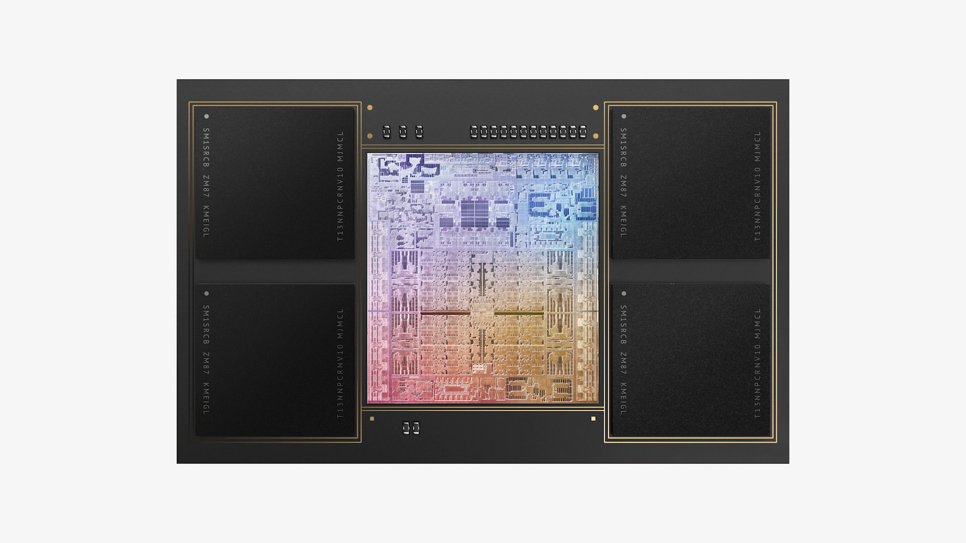
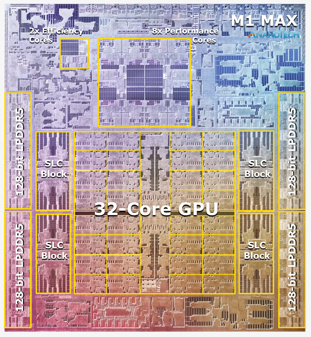
The GPU and memory interfaces of the chip are by far the most differentiated aspects of the chip, instead of a 16-core GPU, Apple doubles things up to a 32-core unit. On the M1 Max which we tested for today, the GPU is running at up to 1296MHz - quite fast for what we consider mobile IP, but still significantly slower than what we’ve seen from the conventional PC and console space where GPUs now can run up to around 2.5GHz.
Apple also doubles up on the memory interfaces, using a whopping 512-bit wide LPDDR5 memory subsystem – unheard of in an SoC and even rare amongst historical discrete GPU designs. This gives the chip a massive 408GB/s of bandwidth – how this bandwidth is accessible to the various IP blocks on the chip is one of the things we’ll be investigating today.
The memory controller caches are at 48MB in this chip, allowing for theoretically amplified memory bandwidth for various SoC blocks as well as reducing off-chip DRAM traffic, thus also reducing power and energy usage of the chip.
Apple’s die shot of the M1 Max was a bit weird initially in that we weren’t sure if it actually represents physical reality – especially on the bottom part of the chip we had noted that there appears to be a doubled up NPU – something Apple doesn’t officially disclose. A doubled up media engine makes sense as that’s part of the features of the chip, however until we can get a third-party die shot to confirm that this is indeed how the chip looks like, we’ll refrain from speculating further in this regard.


493 Comments
View All Comments
techconc - Monday, October 25, 2021 - link
I guess you missed the section where they showed the massive performance gains for the various content creation applications.GatesDA - Monday, October 25, 2021 - link
Apple currently has the benefit of an advanced manufacturing process. If it feels like future tech compared to Intel/AMD, that's because it is. The real test will be if it still holds up when x86 chips are on equal footing.Notably, going from M1 Pro to Max adds more transistors than the 3080 has TOTAL. This wouldn't be feasible without the transistor density of TSMC's N5 process. M1's massive performance CPU cores also benefit from the extra transistor density.
Samsung and Intel getting serious about fabrication mean it'll be much harder for future Apple chips to maintain a process advantage. From the current roadmaps they'll actually fall behind, at least for a while.
michael2k - Monday, October 25, 2021 - link
That's a tautology and therefore a fallacy and bad logic:Apple is only ahead because they're ahead. When they fall behind they will fall behind.
You can deconstruct your fallacy by asking this:
When will Intel get ahead of Apple? The answer is never, at least according to Intel itself:
https://appleinsider.com/articles/21/03/23/now-int...
By the time Intel has surpassed TSMC, it means Intel will need to have many more customers to absorb the costs of surpassing TSMC, because it means Intel's process advantage will be too expensive to maintain without the customer base of TSMC.
kwohlt - Tuesday, October 26, 2021 - link
It's pretty clear that Apple will never go back to x86/64, and that they will be using in-house designed custom silicon for their Macs. Doesn't matter how good AMD or Intel get, Apple's roadmap on that front is set in stone for as far into the future as corporate roadmaps are made.Intel saying they hope to one day get A and M series manufacturing contracts suggests they're confident about their ability to rival TSMC in a few years, not that they will never be able to reach Apple Silicon perf/watt.
Intel def won't come close to M series in perf/watt until at least 2025 with Royal Core Project, and even then, who knows, still probably not.
daveinpublic - Monday, October 25, 2021 - link
So by your logic, Apple is ahead right now.Samsung and Intel are behind right now. And could be for a while.
Sunrise089 - Tuesday, October 26, 2021 - link
The Apple chips have perf/watt numbers in some instances 400% better than the Intel competition. Just how much benefit are you expecting a node shrink to provide? Are you seriously suggesting Intel would see a doubling, tripling, or even quadrupling of perf/watt via moving to a smaller node? You are aware node shrink efficiency gains don’t remotely approach that level of improvement be it on Intel or TSMC, aren’t you?“Samsung and Intel getting serious about fabrication.” What does this even mean? Intel has been the world leader in fabrication investment and technology for decades before recently falling behind. How on earth could you possibly consider them not ‘serious’ about it?
AshlayW - Tuesday, October 26, 2021 - link
Firestorm cores have >2X the transistors as Zen3/Sunny Cove cores in >2X the area on the same process (or slightly less). The cores are designed to be significantly wider making use of the N5 process, and yes, I very much expect at LEAST a doubling of perf/w from N5 CPUs from AMD, since they doubled Ryzen 2000 with 3000, and +25% from 3000 to 5000 on the same N7 node.kwohlt - Tuesday, October 26, 2021 - link
Ryzen 3000 doubled perf/watt over Ryzen 2000?? Which workloads on which SKUs are you comparing?dada_dave - Monday, October 25, 2021 - link
So I wonder why Geekbench scores have so far shown M1Max very far off it's expected score relative to the M1 (22K)? I've checked other GPUs in its score range across a variety of APIs (including Metal) and so far they all show the expected scaling (or close enough) between TFLOP and GB score except the M1 Max. Even the 24 core Max is not that far off, it's the 32 core scores are really far off. They should be in the 70Ks or even high 80Ks for perfect scaling which is achieved by the 16-core Pro GPU, but the 32-core scores are actually in the upper 50Ks/low 60Ks. Do you have any hypotheses as to why that is? Also does the 16" have the high performance mode supposedly coming (or here already)?Andrei Frumusanu - Monday, October 25, 2021 - link
The GB compute is too short in bursts and the GPU isn't ramping up to peak frequencies. Just ignore it.