The Ampere Altra Review: 2x 80 Cores Arm Server Performance Monster
by Andrei Frumusanu on December 18, 2020 6:00 AM EST- Posted in
- Servers
- Neoverse N1
- Ampere
- Altra
Test Bed and Setup - Compiler Options
For the rest of our performance testing, we’re disclosing the details of the various test setups:
Ampere "Mount Jade" - Dual Altra Q80-33
Obviously, for the Ampere Altra system we’re using the provided Mount Jade server as configured by Ampere.
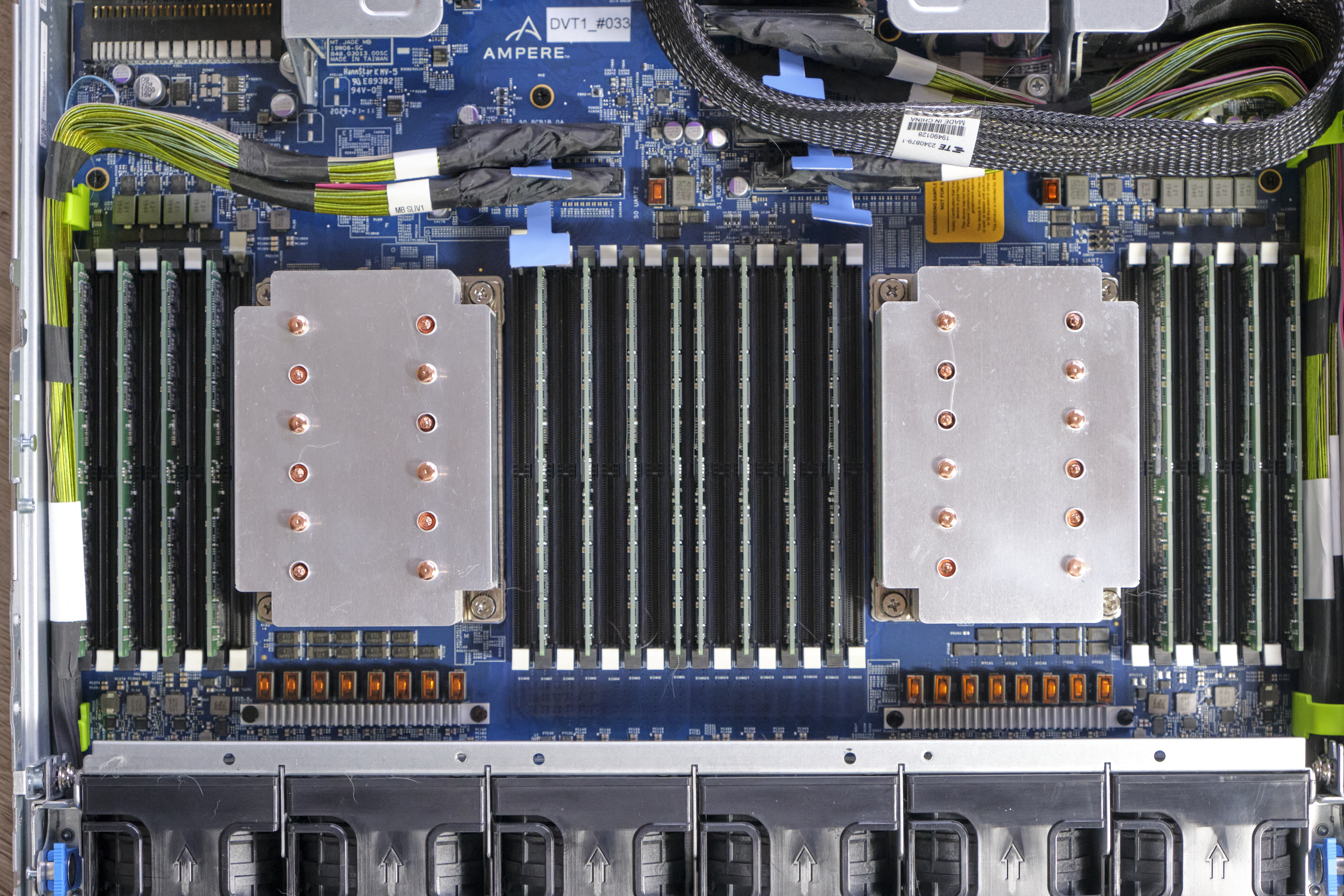
The system features 2 Altra Q80-33 processors within the Mount Jade DVT motherboard from Ampere.
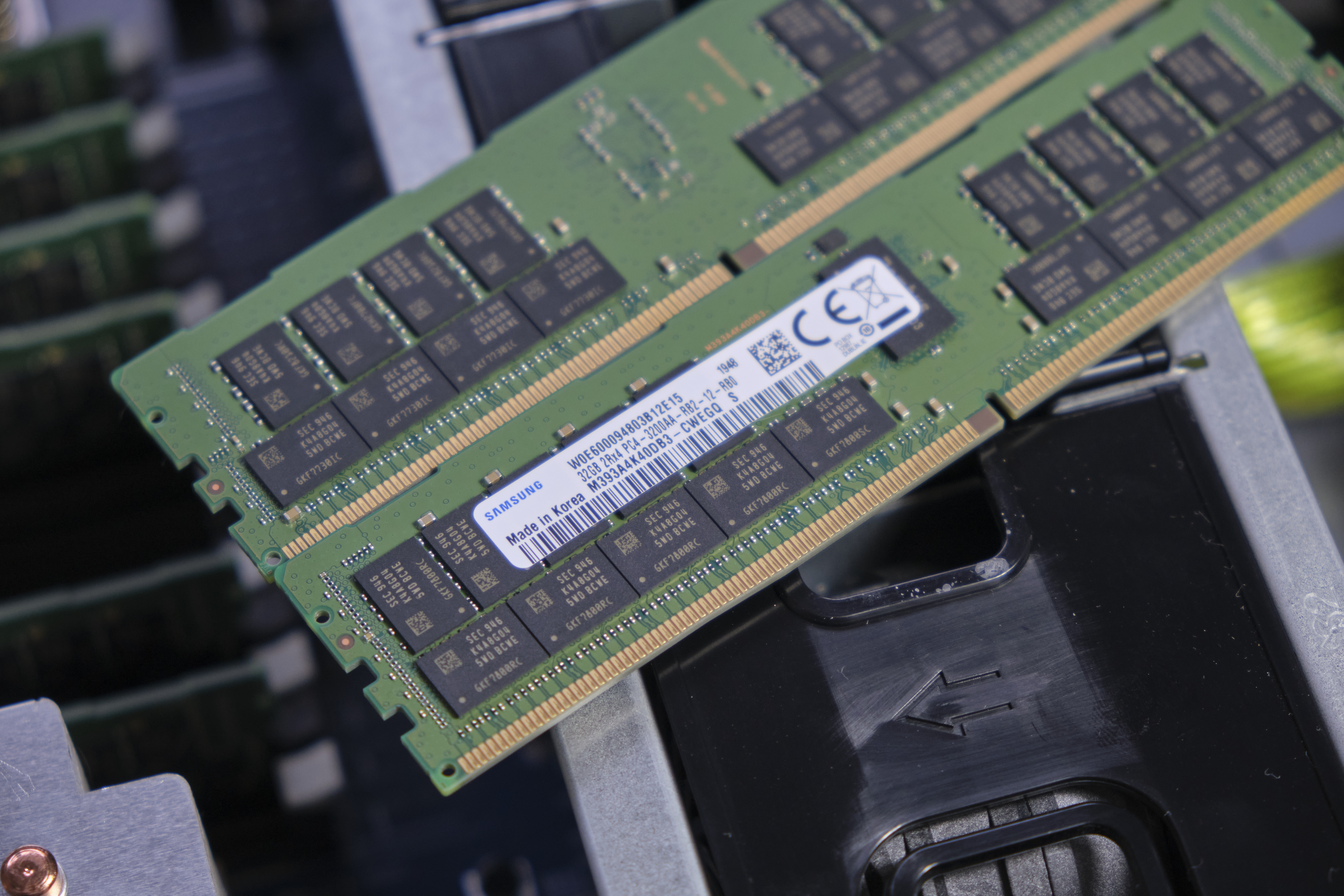
In terms of memory, we’re using the bundled 16 DIMMs of 32GB of Samsung DDR4-3200 for a total of 512GB, 256GB per socket.
| CPU | 2x Ampere Altra Q80-33 (3.3 GHz, 80c, 32 MB L3, 250W) |
| RAM | 512 GB (16x32 GB) Samsung DDR4-3200 |
| Internal Disks | Samsung MZ-QLB960NE 960GB Samsung MZ-1LB960NE 960GB |
| Motherboard | Mount Jade DVT Reference Motherboard |
| PSU | 2000W (94%) |
The system came preinstalled with CentOS 8 and we continued usage of that OS. It’s to be noted that the server is naturally Arm SBSA compatible and thus you can run any kind of Linux distribution on it.
Ampere makes special note of Oracle’s active support of their variant of Oracle Linux for Altra, which makes sense given that Oracle a few months ago announced adoption of Altra systems for their own cloud-based offerings.
The only other note to make of the system is that the OS is running with 64KB pages rather than the usual 4KB pages – this either can be seen as a testing discrepancy or an advantage on the part of the Arm system given that the next page size step for x86 systems is 2MB – which isn’t feasible for general use-case testing and something deployments would have to decide to explicitly enable.
The system has all relevant security mitigations activated, including SSBS (Speculative Store Bypass Safe) against Spectre variants.
AMD - Dual EPYC 7742
For our AMD system, unfortunately we had hit some issues with our Daytona reference server motherboard, and moved over to a test-bench setup on a SuperMicro H11DSI0.
We’re also equipping the system with 256GB per socket of 8-channel/DIMM DDR4-3200 memory, matching the Altra system.
| CPU | 2x AMD EPYC 7742 (2.25-3.4 GHz, 64c, 256 MB L3, 225W) |
| RAM | 512 GB (16x32 GB) Micron DDR4-3200 |
| Internal Disks | OCZ Vector 512GB |
| Motherboard | SuperMicro H11DSI0 |
| PSU | EVGA 1600 T2 (1600W) |
As an operating system we’re using Ubuntu 20.10 with no further optimisations. In terms of BIOS settings we’re using complete defaults, including retaining the default 225W TDP of the EPYC 7742’s, as well as leaving further CPU configurables to auto, except of NPS settings where it’s we explicitly state the configuration in the results.
The system has all relevant security mitigations activated against speculative store bypass and Spectre variants.
Intel - Dual Xeon Platinum 8280
For the Intel system we’re also using a test-bench setup with the same SSD and OS image actually – we didn’t have enough RAM to run both systems concurrently.
Because the Xeons only have 6-channel memory, their maximum capacity is limited to 384GB of the same Micron memory, running at a default 2933MHz to remain in-spec with the processor’s capabilities.
| CPU | 2x Intel Xeon Platinum 8280 (2.7-4.0 GHz, 28c, 38.5MB L3, 205W) |
| RAM | 384 GB (12x32 GB) Micron DDR4-3200 (Running at 2933MHz) |
| Internal Disks | OCZ Vector 512GB |
| Motherboard | ASRock EP2C621D12 WS |
| PSU | EVGA 1600 T2 (1600W) |
The Xeon system was similarly run on BIOS defaults on an ASRock EP2C621D12 WS with the latest firmware available.
The system has all relevant security mitigations activated against the various vulnerabilities.
Compiler Setup
For compiled tests, we’re using the release version of GCC 10.2. The toolchain was compiled from scratch on both the x86 systems as well as the Altra system. We’re using shared binaries with the system’s libc libraries.


148 Comments
View All Comments
Wilco1 - Friday, December 18, 2020 - link
How exactly is it big? It's tiny for a server chip - 80 cores at about half the die size of a typical 28-core Xeon (~700mm^2). And TSMC 7nm yield is extremely good even for much larger chips like GPUs.Ithaqua - Friday, December 18, 2020 - link
Plus as with all chips, there may be a 64 / 48 / 32 core version which are just standard chips with the defective core block turned off.eastcoast_pete - Saturday, December 19, 2020 - link
Note I wrote "quite big", and by transistor count, it's a larger CPU, expected for a server chip. As for the Xeon, how high is Intel's yield for the 28 core Xeon, and that after how many years on 14 nm+++ (etc)? So, if you have a yield number for this 80 core Ampere chip, please share it.Wilco1 - Saturday, December 19, 2020 - link
It's larger than a mobile SoC, but small for a server chip thanks to Arm's tiny cores and the high density of TSMC 7nm. See https://www.anandtech.com/show/16028/better-yield-... for the defect rate, and from that a simple yield calculator gives 71% for a 350mm^2 die. That's before you fix SRAM defects or harvest dies for the lower-end SKUs. So we conclude yield is very good.eastcoast_pete - Saturday, December 19, 2020 - link
Glad to read that you've proven Andrei wrong, so maybe you should write these reviews. Here a direct quote from the first page of the review (also, take a look at the pictures: "The chip itself is absolutely humongous and amongst the current publicly available processors is the biggest in the industry, out-sizing AMD’s SP3 form-factor packaging, coming in at around 77 x 66.8mm – about the same length but considerably wider than AMD’s counterparts."Wilco1 - Saturday, December 19, 2020 - link
How ignorant can you be? Obviously the chip and silicon die have different sizes. The chip is large because it has many pins. The silicon die is a tiny fraction of the chip. We're discussing the size of the silicon die here, not the size of the chip. Completely different things.mode_13h - Sunday, December 20, 2020 - link
It'd be less confusing if you'd talk about the "package" dimensions.I think die and chip are traditionally synonymous. For instance, a package with multiple dies is traditionally called a MCM (Multi-Chip Module).
Wilco1 - Monday, December 21, 2020 - link
Look at Andrei's quote above, there isn't a well-defined term - people use chip/CPU/package etc as synonyms.mode_13h - Monday, December 21, 2020 - link
But it's not hard to see how "chip" can cause confusion. So, why not avoid it entirely, and just say either "die" or "package".Only a troll or someone with an agenda could be against clear communication.
Wilco1 - Monday, December 21, 2020 - link
It's hard to imagine how anyone sane can believe that a "chip measuring 77 x 66.8mm" (6 times the reticle limit!) is referring to the die size rather than the package. Andrei's quote even uses the word package. So maybe you're right and eastcoast_pete was just trolling.