A Broadwell Retrospective Review in 2020: Is eDRAM Still Worth It?
by Dr. Ian Cutress on November 2, 2020 11:00 AM ESTPower Consumption
The nature of reporting processor power consumption has become, in part, a dystopian nightmare. Historically the peak power consumption of a processor, as purchased, is given by its Thermal Design Power (TDP, or PL1). For many markets, such as embedded processors, that value of TDP still signifies the peak power consumption. For the processors we test at AnandTech, either desktop, notebook, or enterprise, this is not always the case.
Modern high performance processors implement a feature called Turbo. This allows, usually for a limited time, a processor to go beyond its rated frequency. Exactly how far the processor goes depends on a few factors, such as the Turbo Power Limit (PL2), whether the peak frequency is hard coded, the thermals, and the power delivery. Turbo can sometimes be very aggressive, allowing power values 2.5x above the rated TDP.
AMD and Intel have different definitions for TDP, but are broadly speaking applied the same. The difference comes to turbo modes, turbo limits, turbo budgets, and how the processors manage that power balance. These topics are 10000-12000 word articles in their own right, and we’ve got a few articles worth reading on the topic.
- Why Intel Processors Draw More Power Than Expected: TDP and Turbo Explained
- Talking TDP, Turbo and Overclocking: An Interview with Intel Fellow Guy Therien
- Reaching for Turbo: Aligning Perception with AMD’s Frequency Metrics
- Intel’s TDP Shenanigans Hurts Everyone
In simple terms, processor manufacturers only ever guarantee two values which are tied together - when all cores are running at base frequency, the processor should be running at or below the TDP rating. All turbo modes and power modes above that are not covered by warranty. Intel kind of screwed this up with the Tiger Lake launch in September 2020, by refusing to define a TDP rating for its new processors, instead going for a range. Obfuscation like this is a frustrating endeavor for press and end-users alike.
However, for our tests in this review, we measure the power consumption of the processor in a variety of different scenarios. These include full AVX2/AVX512 (delete as applicable) workflows, real-world image-model construction, and others as appropriate. These tests are done as comparative models. We also note the peak power recorded in any of our tests.
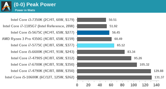
In peak power, the Core i7-5775C sticks to the 65 W value, whereas the Core i5 variant is below its TDP value. This is beyond the 22nm Core i7-4790S which is also a 65 W part.
In real-world tests, first up is our image-model construction workload, using our Agisoft Photoscan benchmark. This test has a number of different areas that involve single thread, multi-thread, or memory limited algorithms.
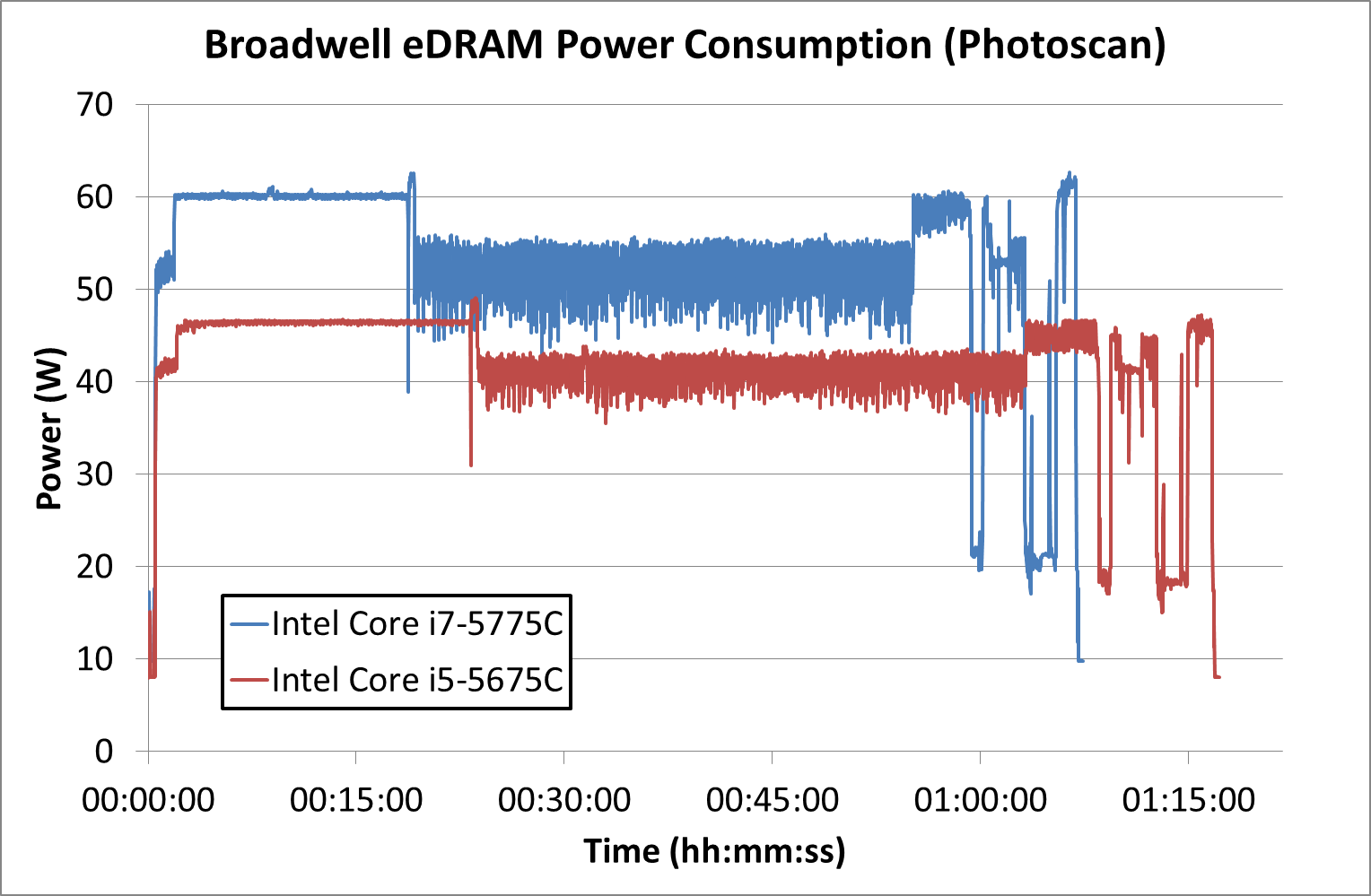
For Photoscan, the Core i7 spends its 'real world' time around 60 W, but does momentarily spike up above that 60 W mark. The Core i5 by comparison doesn't even touch 50 W.
The second test is from y-Cruncher, which is our AVX2/AVX512 workload. This also has some memory requirements, which can lead to periodic cycling with systems that have lower memory bandwidth per core options.
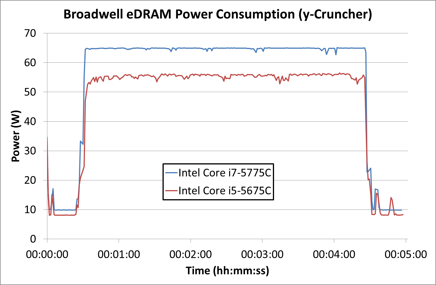
We're seeing some slight variation in power as the y-Cruncher algortihm moves out to DRAM movement over compute, however both processors seem to be hitting either their power limits or just a natural peak power consumption.


120 Comments
View All Comments
Khenglish - Monday, November 2, 2020 - link
The infinity cache is SRAM, which will be faster but much lower density. Only IBM ever integrated DRAM on the same die as a processor. The DRAM capacitor takes up the space where you want to put all your CPU wiring.Quantumz0d - Monday, November 2, 2020 - link
Always thought why Intel is so fucking foolish in making that shitty iGPU die instead of making eDRAM on the chip. It would have given a massive boost for all their CPUs. A big missed opportunity. AMD had this "Game cache" on their Zen 2 and now with RDNA2, "Infinity Cache" again..jospoortvliet - Wednesday, November 4, 2020 - link
I guess they did the math on cost and power. They always had better memory controllers and prefetchers so they didn't benefit as much from cache- they also have the memory controller on-die, unlike amd with their i/o die. So intel would benefit waaaay less than amd does, in almost every way.dragosmp - Monday, November 2, 2020 - link
"...the same 22nm eDRAM chip is still in use today with Apple's 2020 base Macbook Pro 13"Ahem, what? Is that CPU an off the roadmap Tiger Lake?
Jorgp2 - Monday, November 2, 2020 - link
Tiger Lake doesn't have the hardware for an L4.It's probably the Skylake version
colinisation - Monday, November 2, 2020 - link
Do the part numbers on Intel CPU's mean anything, I picked up a 5775C a week agoand have not installed it yet but the part number starts "L523" - I just assume it is a later batch than what is in the review.ilt24 - Tuesday, November 3, 2020 - link
@colinisationThat L523 are the first 4 characters of the is the Finished Process Order or Batch#.
The L says it was packaged in Malaysia
The 5 says it was packaged in 2015
The 23 says it was packaged on the 23rd week
Digits 5-8 are the specific lot number number of the wafer the die came from
colinisation - Tuesday, November 3, 2020 - link
@ilt24 - Thank you very muchMday - Monday, November 2, 2020 - link
I expected more eDRAM implementations after Broadwell coming from Intel and AMD on the CPU side, as a low latency - high "capacity" cache, particularly after the launch of HBM. It made me wonder why Intel even bothered, or what shifts in strategies moved them to and away from eDRAM.ichaya - Monday, November 2, 2020 - link
This is really the first desktop part I'm hearing of, weren't most of these "Iris Pro" chips sold in Apple laptops with maybe a small minority being sold by other laptop OEMs? I believe so.