Intel’s Tiger Lake 11th Gen Core i7-1185G7 Review and Deep Dive: Baskin’ for the Exotic
by Dr. Ian Cutress & Andrei Frumusanu on September 17, 2020 9:35 AM EST- Posted in
- CPUs
- Intel
- 10nm
- Tiger Lake
- Xe-LP
- Willow Cove
- SuperFin
- 11th Gen
- i7-1185G7
- Tiger King
10nm SuperFin, Willow Cove, Xe, and new SoC
Inside Intel’s 11th Generation ‘Tiger Lake’ processor are four ‘Willow Cove’ cores, 96 Execution Units of graphics built with the Xe-LP microarchitecture, all on top of Intel’s latest 10nm SuperFin manufacturing technology. Because each part of this processor has had updates, even trying to explain it in a single sentence can be cumbersome. For the most part, Intel has covered a number of details relating to all these features across the events in August and September – at Intel’s Architecture Day 2020 and the 11th Gen Core announcement, which we will recap here before going into our own testing.
Our full articles on this information can be found at:
- Intel’s 11th Gen Core Tiger Lake SoC Detailed: SuperFin, Willow Cove and Xe-LP
- Intel Launches 11th Gen Core Tiger Lake: Up to 4.8 GHz
10nm SuperFin
Intel’s Tiger Lake design has been enabled through its latest manufacturing process node update. This is a new version of Intel’s 10nm process, and Intel claims that this update is akin to a ‘full node transition’, as if Intel was offering a new manufacturing process altogether. To back up this claim, Intel says that the new generation 10nm offers 17-18% better transistor performance compared to the previous generation 10nm, equivalent to the four updates it applied to 14nm over several years but at the same time. This is a good thing – better performance, a wider frequency and voltage window, and potentially better density, all while using the same manufacturing hardware.
Intel is calling its new process node enhancement ‘SuperFin’, based two of the key design changes that the company has used.
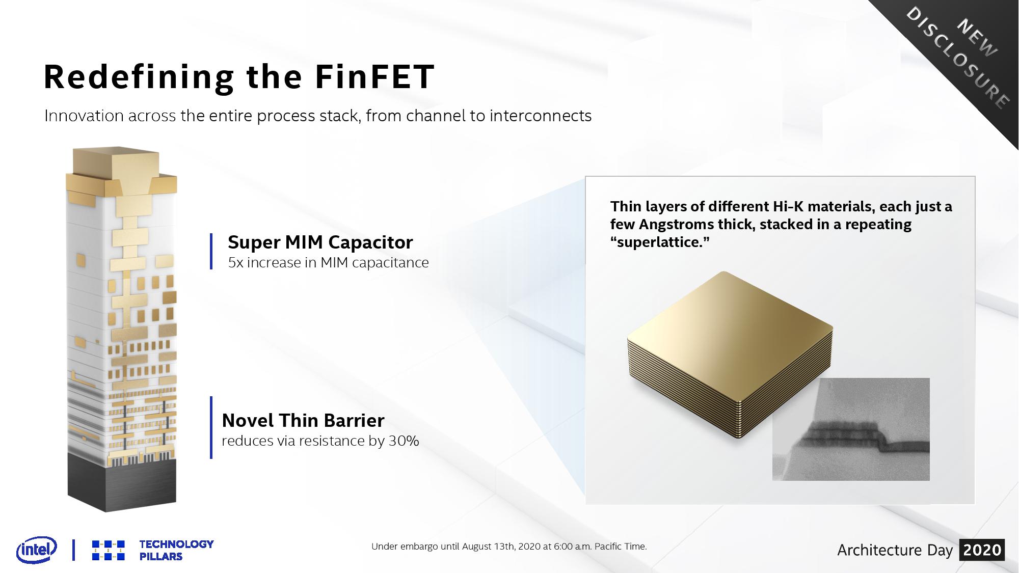
At the lower layers of the stack, Intel is introducing a new set of barrier materials to enable thinner barriers, which also helps reduce resistance of vias by up to 30% by enabling the metal each via to be a bigger proportion of the fixed size. Reducing the resistance enhances the performance of the interconnect between the metal layers
At the higher levels, Intel is introducing a new SuperMIM (metal-insulator-metal) capacitor. Intel states that this new design gives a 5x increase in capacitance over an industry standard MIM cap within the same footprint. This drives a voltage reduction that ultimately leads to drastically improved product and transistor performance. Intel states that this is an industry first/leading design, enabled through careful deposition of new Hi-K materials in thin layers, smaller than 0.1nm, to form a superlattice between two or more material types.
On top of this, a new high-performance third generation FinFET design, enabled through a better gate-generation process and lower resistance source/drain, is what Intel has stated will enable future products. All combined, against a base 10nm process (Intel doesn’t specify which, although most analysts assume this is Cannon Lake, the OG 10nm), Intel is promoting 17-18% better transistor performance with the SuperFin.
Going forward, all products built on this process are going to be called ‘10nm SuperFin’. In the original 10nm parlance, this was 10++. Note that 10++ was renamed 10+ back at CES 2020, and so this is the second renaming. To avoid any confusion, Intel has provided a decoder ring to keep everyone up to date:
- (Pre-10nm: Cannon Lake)
- 10nm: Ice Lake Notebook, Ice Lake Xeon, Snow Ridge
- 10nm SuperFin: Tiger Lake, Xe-LP Products (DG1, SG1)
- 10nm Enhanced Superfin: Sapphire Rapids Xeon, Xe-HP Products (1-4 Tile)
After 10ESF we should see Intel move into its 7nm process and products.
Tiger Lake: Willow Cove
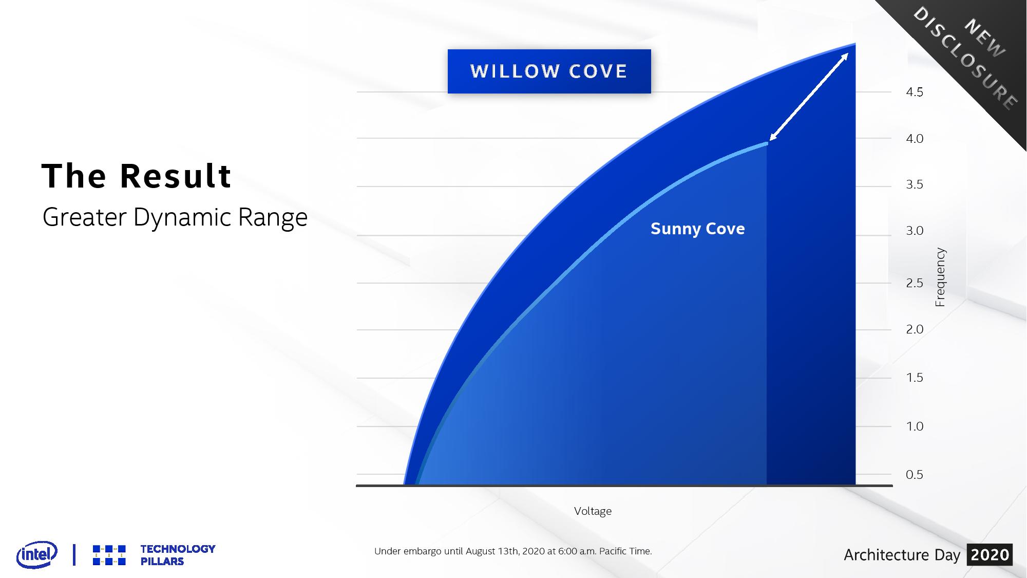
The new microarchitecture of the main CPU cores is called Willow Cove, and is an update over the previous generation Sunny Cove. Intel claims a 10-20% performance improvement generation on generation, however it is important to understand that this is not a raw clock-for-clock gain but rather a peak performance claim.
In terms of a clock-for-clock gain, Intel by and large has said in our technical briefings that Willow Cove will only have minor improvements due to the cache structure (more on that below). Aside from the cache, there are a few changes to deal with security and side-channel attacks, but no other changes to the core design to note. We did discover a few performance updates to specific instructions, which we’ll go into later in the review, but essentially unless the core is L2/L3 cache sensitive, users should not expect to see a clock-for-clock performance difference.
Where Tiger Lake’s 10-20% performance uplift comes from is both performance efficiency and peak performance. Because of the SuperFin design, and a new high-performance transistor library, Intel claims to have enabled the Willow Cove core to be more efficient at every frequency compared to the previous generation, but also extend the frequency range. Where the previous generation was limited to around 4.0 GHz, the new Tiger Lake as launched can go to 4.8 GHz. Based on our discussions with Intel’s engineers, it can go even higher.
Aside from the frequency adjustment, the biggest change inside the core is the cache hierarchy.
The private L2 cache gets the biggest update, with a +150% increase in size. Traditionally increasing the cache size by double will decrease the miss rate by √2, so the 2.5x increase should reduce L2 cache misses by ~58%. The flip side of this is that larger caches often have longer access latencies, so we would expect the new L2 to be slightly slower. After many requests, Intel said that its L2 cache was a 14-cycle latency, which we can confirm, making it only +1 cycle over the previous generation. It’s quite impressive to more than double a cache size and only add one cycle of latency. The cache is also now a non-inclusive cache.
The L3 also gets an update, in two ways. The size has increased for the highest core count processors, from 2 MB per core to 3 MB per core, which increases the L3 cache line hit rate for memory accesses. However, Intel has reduced the associativity from 16-way at 8 MB per 4C chip to 12-way at 12 MB per 4C chip, which reduces the cache line hit rate, but improves the power consumption and the L3 cache latency. There is some L3 latency cycle loss overall, however due to the size increase Intel believes that there is a net performance gain for those workloads that are L3-capacity bottlenecked.
| Cache Comparison for Mobile CPUs | |||||
| AnandTech | Coffee Lake 4C |
Ice Lake 4C |
Tiger Lake 4C |
AMD Zen2 4C |
|
| L1-I | 32 KiB 8-way |
32 KiB 8-way |
32 KiB 8-way |
32 KiB 8-way |
|
| L1-D | 32 KiB 8-way 4-cycle |
48 KiB 12-way 5-cycle |
48 KiB 12-way 5-cycle |
32 KiB 8-way 4-cycle |
|
| L2 | 256 KiB 4-way 12-cycle Inclusive |
512 KiB 8-way 13-cycle Inclusive |
1.25 MiB 20-way 14-cycle* Non-Inc |
512 KiB 8-way 12-cycle Inclusive |
|
| L3 | 8 MiB 16-way 42-cycle Inclusive |
8 MiB 16-way 36-cycle Inclusive |
12 MiB 12-way 43-cycle* Non-Inc |
8 MiB 16-way 34-cycle Non-Inc |
|
| *As measured new for this review | |||||
For most users, the adjustment in cache sizes and latency should not be specifically noticeable. In discussing with Intel, they recognize that some specific workloads will benefit, however these changes were made from a higher-level SoC design viewpoint. We are of the opinion that this might have been done to help with the manufacturing, or thermal density, or may lead into future products. Intel, like other companies, does perform a lot of customer workload analysis about where the cache bottlenecks are, ultimately designing the next generation of cores to serve what it assumes will be the major workload mix when it comes to market.
Tiger Lake: Xe-LP
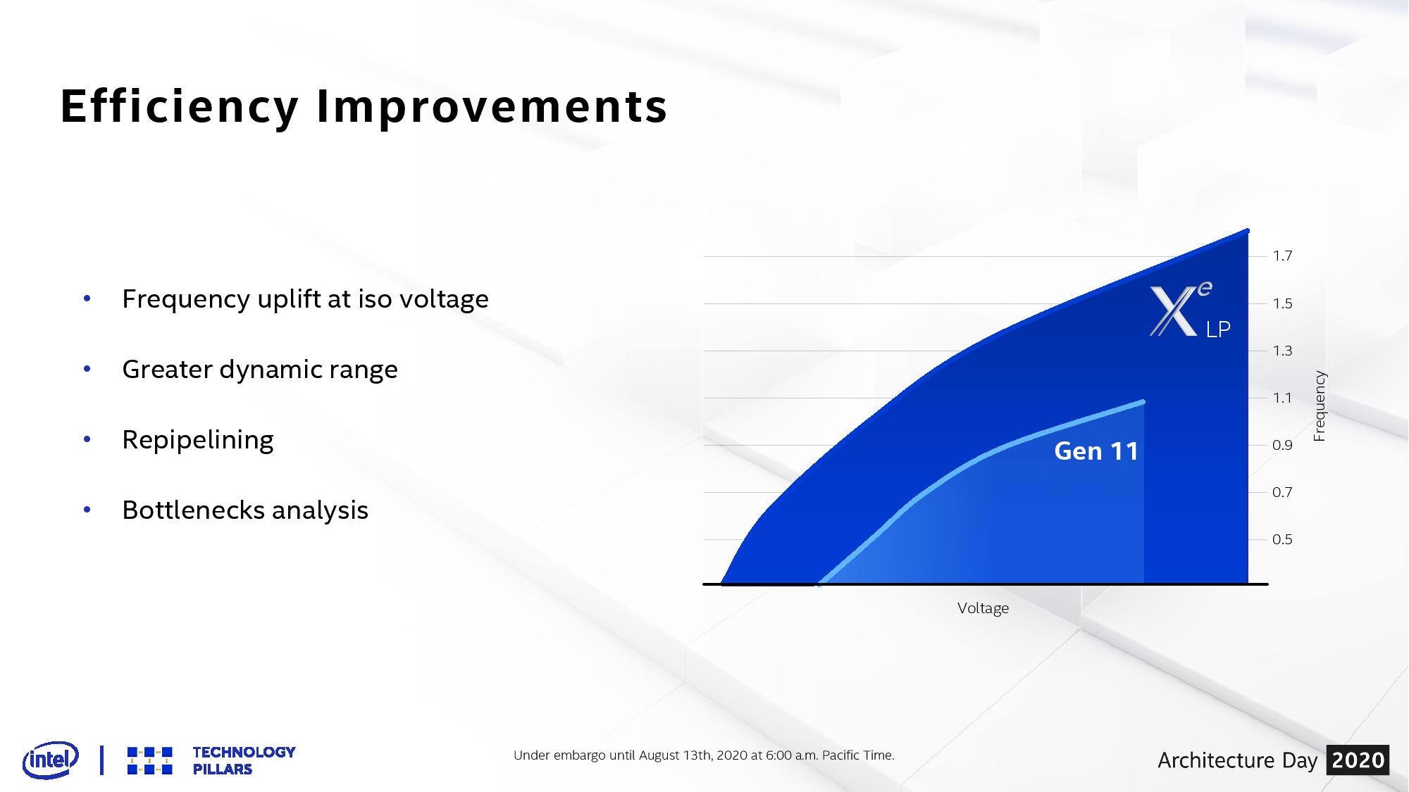
A big part of the Tiger Lake/Ice Lake comparison will be the performance difference in graphics. Where Ice Lake has 64 Execution Units of Gen11 graphics, Tiger Lake has 96 Execution Units but of the new Xe-LP architecture. On top of that, there’s the new SuperFin transistor stack that promises to drive frequencies (and power windows) a lot higher, making Tiger Lake more scalable than before. Where Gen11 graphics saw frequencies up to 1100 MHz, the initial Xe-LP designs with Tiger Lake are at 1450 MHz. Intel has teased that future versions of Xe-LP (likely the discrete DG1 card) will go up to 1750-1800 MHz.
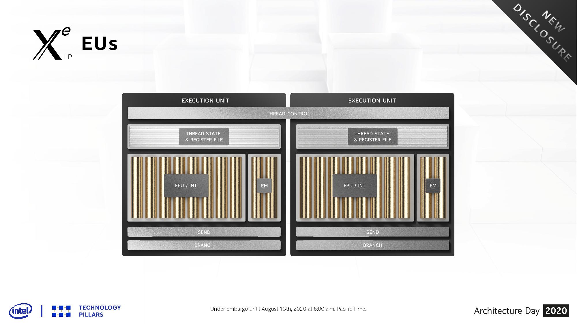
Within Intel’s graphics cores, we speak about ALUs, or Arithmetic Logic Units. These ALUs can often do a number of things, such as math on integers (whole numbers), math on floating point numbers (fractions), or extended math (such as trigonometry).
In the Ice Lake Gen11 graphics system, each one of the 64 execution units consisted of an 8 ALU design with one set of four for FP/INT, and the other set of four for FP/Extended Math.
For Xe-LP, each of the 96 execution units have 10 ALUs, and they are split differently: the first 8 are for FP/INT, and the last 2 are for extended math. The 8 FP/INT in the new graphics support both INT16 (at double rate) and INT32 data types as well as new DP4a instructions can accelerate INT8 inference workloads. The new execution units also now work in pairs – two EUs will share a single thread control block to help assist with coordinated workload dispatch.
The graphics has its own L3 cache as well, which has a junction on the ring interconnect used inside Tiger Lake. In order to help accelerate graphics workloads further, Intel has doubled the bandwidth of the ring interconnect by essentially giving the SoC two rings, supporting 2x32B/cycle transfers bidirectionally.
Overall Intel is claiming up to 2x graphics throughput with the new Xe-LP compared to previous Gen11. Moving from 64 EUs to 96 EUs would immediately give +50% performance, and then the increase from 1100 MHz to 1450 MHz is another 32%. Together they would account for a 98% throughput increase, all other things scaling equally (memory bandwidth and such).
Tiger Lake: Media and Display
Tiger Lake will be Intel’s first official support for the AV1 codec in decode mode, and Intel has also doubled its encode/decode throughput for other popular codecs. This means a full hardware-based 12-bit video pipeline for HDR and 8K60 playback support.
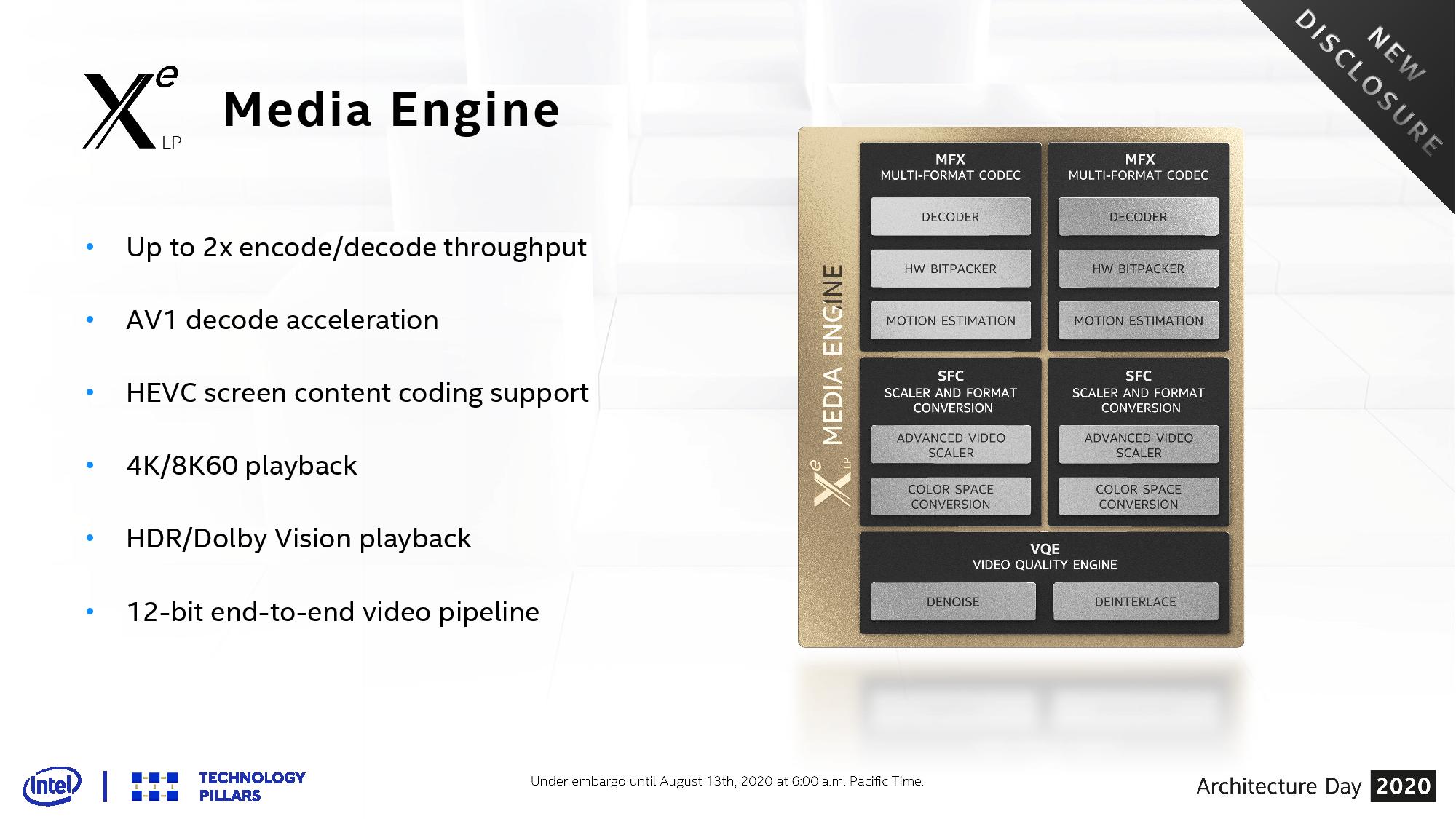
Display Support for Tiger Lake is also extended with four 4K display pipelines. Connections over DP1.4, HDMI 2.0, Thunderbolt 4, and USB4 Type-C simultaneously is how Intel expects users to operate if all four outputs are needed at once. The display engine also supports HDR10, 12-bit BT2020 color, Adaptive Sync, and support for monitors up to 360 Hz.
Other SoC Adjustments
There are a few other elements about Tiger Lake that are known at an SoC level that should also be noted.
Tiger Lake now has support for LPDDR4X-4266 (32 GB max) as well as DDR4-3200 (64 GB max), which is a slight improvement over the previous generation Ice Lake on the LPDDR4X side. The silicon is also designed to support LPDDR5-5400, however we are unlikely to see any devices with LPDDR5 until the new year due to the extra validation requirements and the current extra cost that LPDDR5 brings. Intel discussed with its partners, and they preferred that Intel prioritized LPDDR4X validation to begin with. We have been told by Intel that LPDDR5 support on the current silicon, pending full validation, does not require a new silicon stepping.
Also related to memory, the new silicon now supports Total Memory Encryption. TME has been a popular feature of new silicon designs of late, and enables mobile device users to have the data held in the memory on a system physically secure against hardware attacks. In other systems we’ve been told that a feature like TME, when implemented correctly, only gives a 1-2% performance hit in the most usual worst case – Intel has not provided equivalent numbers as of yet. Given the type of feature this is, we suspect TME might be more of a vPro-enabled product feature, however we will have to get clarity on that.
One question that everyone likes to ask is die size. We took out some calipers and measured 13.49 x 10.70 mm = 144.34 mm2. This is rather close to our estimate from CES from the wafer photographs, where we guessed 146.10 mm2 (~1.2% error).
| Die Sizes | ||||||
| AnandTech | x | y | Die Size | Process | Cores | EUs/ CUs |
| AMD Zen 2 Chiplet | 10.32 | 7.34 | 75.75 mm2 | TSMC N7 | 8 | - |
| Intel Ice Lake | 11.44 | 10.71 | 122.52 mm2 | Intel 10 | 4 | 64 |
| Intel Tiger Lake | 13.49 | 10.70 | 144.34 mm2 | Intel 10SF | 4 | 96 |
| AMD Picasso | 19.21 | 10.92 | 209.78 mm2 | GF 12 | 4 | 11 |
| AMD Renoir APU | 13.59 | 10.98 | 149.22 mm2 | TSMC N7 | 8 | 8 |
There are also security features, which we will cover in the next page.


253 Comments
View All Comments
huangcjz - Thursday, September 17, 2020 - link
No, you can say "have to hand" as in something which is available. E.g. "Do you have the presentation to hand?"29a - Thursday, September 17, 2020 - link
Wouldn't a non Iris chip be a fairer comparison to Renoir?Kamen Rider Blade - Thursday, September 17, 2020 - link
AMD's 4800U has a 25 watt mode, Hardware UnBoxed tested it against Intel.Why didn't you test it and put those results in the chart?
Why this biased reviewing of one side gets 15 watt and 28 watt scores.
Yet AMD isn't allowed to show 25 watt scores?
What are you afraid of when comparing like for like?
IanCutress - Thursday, September 17, 2020 - link
For us, the 15W to 15W results were the focal point. 28W is there to show a max Intel and look at scaling. Also, The amount of 4800U devices at 25W is minimal.Not only that, I'm on holiday. I had to spend two days out, while in this lovely cottage in the countryside, to write 18k words, rather than spend time with my family. I had 4 days with the TGL laptop, and 8 days notice in advance to prepare before the deadline. Just me with a couple of pages from Andrei, no-one else. Still posted the review 30 minutes late, while writing it in a pub as my family had lunch. Had to take the amd laptop with me to test, and it turns out downloading Borderlands 3 in the middle of nowhere is a bad idea.
Not only that, I've been finishing up other projects last week. I do what I can in the time I have. This review is 21k words and more detailed than anything else out there done by a single person currently in the middle of a vacation. If you have further complains, our publisher's link is at the bottom of the webpage. Or roll your own. What are you afraid of? I stand by my results and my work ethic.
PixyMisa - Thursday, September 17, 2020 - link
I really appreciate the effort. The individual SPEC results are vastly more useful than (for example) a single Geekbench score.Spunjji - Friday, September 18, 2020 - link
I can second that - I appreciate seeing a breakdown of the strengths/weaknesses of each core design.Kamen Rider Blade - Friday, September 18, 2020 - link
We appreaciate your hard work, I do watch your YT channel Tech Tech Potato. That being said, if you knew about this issue, with not comparing like for like; then just omit the 28 W scores from the Intel machine and just focus on Intel's 15W vs AMD's 15W.Why even include the 28W on the chart? You know how this makes you and Anandtech look, right? The issues of bias towards or against any entity could've been easily avoided if you had "Like for like" scores across the board. That's part of what Steve from Gamers Nexus and many of us enthusiast see's as "Bias Marketing" or "Paid Shilling" to manipulate results in one way or another. Many people can easily interpret your data of not showing "like for like" in many wrong ways when they have no context for it.
If you didn't want to test AMD's 25 watt scores, nobody would care, just don't bring up Intel's equivalent 28 watt scores. Alot of the more casual readers won't look at the details and they can easily mis-interpret things. I prefer that your good name doesn't get dragged down in mud with a simple omission of certain benchmark figures. I know you wouldn't deliberately do that to show bias towards one entity or another, but will other folks know that?
Spunjji - Friday, September 18, 2020 - link
Presenting the figures he has isn't bias. Bias would be proclaiming Intel to be the winner without noting the discrepancy, or specifically choosing tests to play to the strength of one architecture.As it is, the Lenovo device doesn't do a 25W mode, so you're asking him to add a full extra device's worth of testing to an already long review. That's a bit much.
If you take a look at the 65W APU results and compare them, you'll see a familiar story for Renoir - there's not actually a whole lot of extra gas in the tank to be exploited by a marginally higher TDP. It performs spectacularly well at 15W, and that's that.
Kamen Rider Blade - Friday, September 18, 2020 - link
You can literally just omit the 65W APU, it has no relevance to be on that chart.Ok, if that Lenovo LapTop doesn't offer a 25W mode, fine. Maybe Hardware Unboxed got a different model of LapTop for the 4800U. Then don't present Intel's 28W mode.
That's how people misunderstand things when there is a deliberate omission of information or extra information that the other side doesn't happen. The lack of pure like for like causes issues.
Spunjji - Saturday, September 19, 2020 - link
You're *demanding bias*. They had the Intel device with a 28W mode, 28W figures are a big part of the TGL proposition, so they tested it and labelled it all appropriately. That isn't bias.The "lack of pure like for like" only causes issues if you don't really pay attention to what the article says about what they had and how they tested it.