Intel's 10nm Cannon Lake and Core i3-8121U Deep Dive Review
by Ian Cutress on January 25, 2019 10:30 AM ESTCPU Performance: Memory and Power
Memory
With the same memory setup as the standard Skylake-style core, without any other improvements, we should expect Cannon Lake to perform exactly similar. Here’s a recap of the memory configuration:
| Memory Comparison | ||
| Skylake Desktop | Cannon Lake | |
| L1-D Cache |
32 KiB/core 8-way |
32 KiB/core 8-way |
| L1-I Cache |
32 KiB/core 8-way |
32 KiB/core 8-way |
| L2 Cache |
256 KiB/core 4-way |
256 KiB/core 4-way |
| L3 Cache |
2 MiB/core 16-way |
2 MiB/core 16-way |
| L3 Cache Type | Inclusive | Inclusive |
For this test we put our Cannon Lake and Kaby Lake processors through our Memory Latency Checker test. Both systems had turbo modes disabled, forcing them to run at 2.2 GHz for parity and a direct microarchitecture comparison.
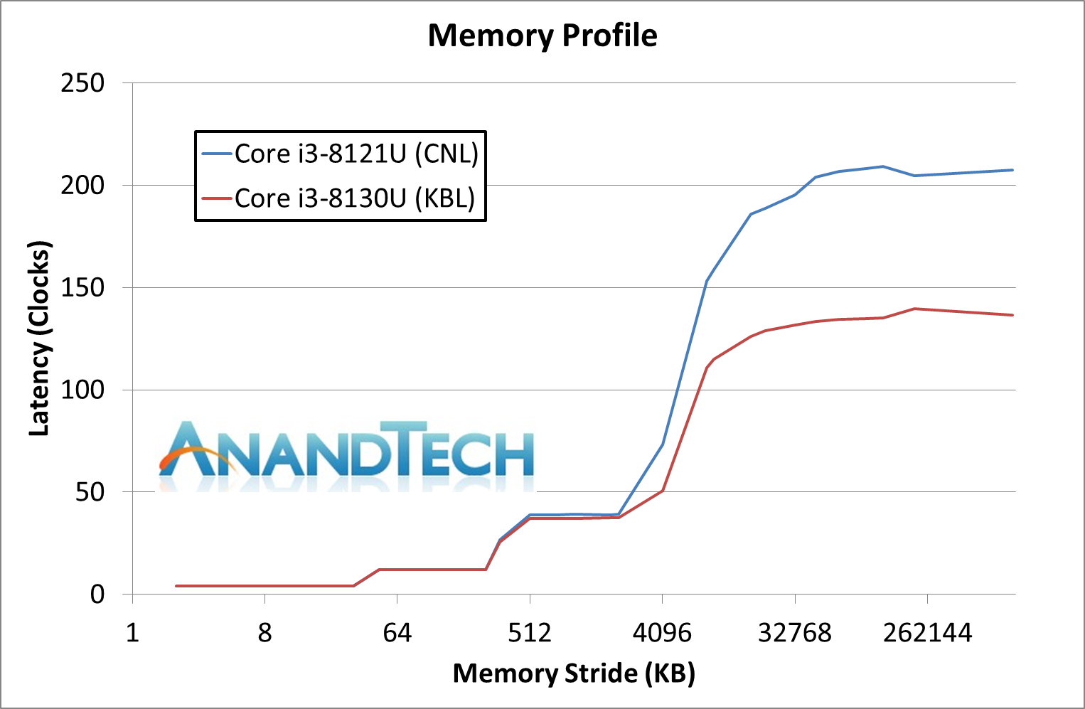
In this instance we see very little different between the two through the caches of the chip. Up to about 2MiB, both chips perform practically identical. Beyond this however, going out to main memory, there is a big discrepancy between the Kaby Lake and the Cannon Lake processor. In essence, accessing Cannon Lake main memory has an additional 50% latency.
At first we thought this was a bug. For both systems to have dual channel memory and running DDR4-2400, something had to be wrong. We double checked the setups – both systems were running in dual channel mode, giving the same memory bandwidth. The Cannon Lake processor was running at DDR4-2400 17-17-17, whereas the Kaby Lake system was at DDR4-2400 16-16-16 (due to memory SPD differences), which isn’t a big enough change to have such a big difference. The only reason we can come up with is that the memory controller on Cannon Lake must have additional overhead from the core to the memory controller – either a slower than expected PLL or something.
Power
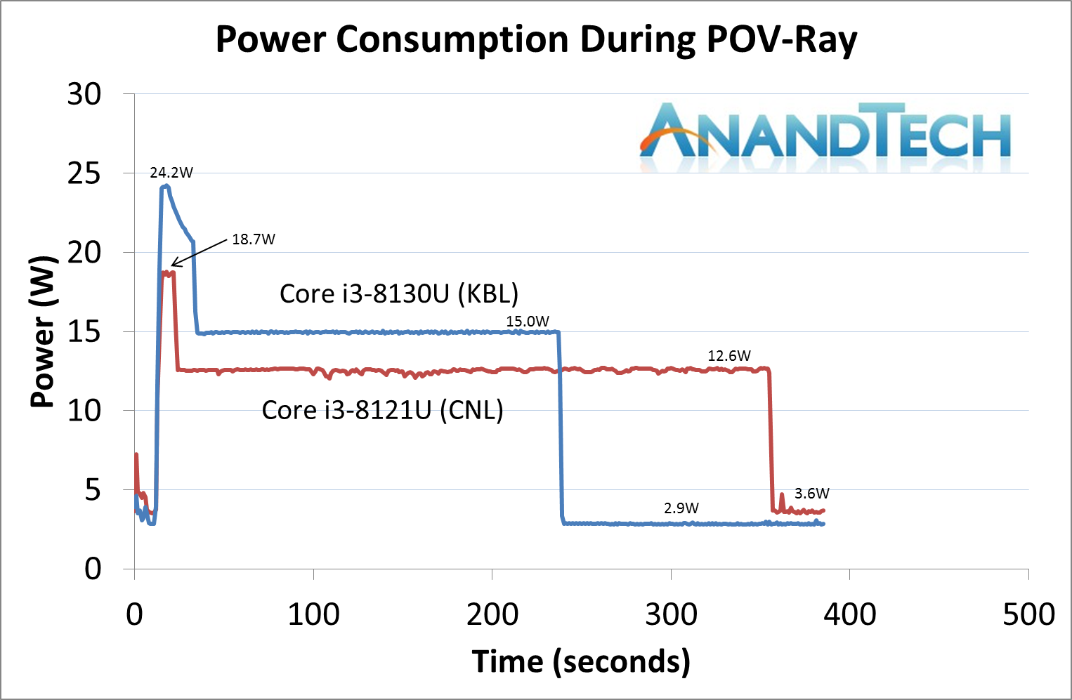
Measuring the power of these thermally limited systems is somewhat frustrating in that we are at the whims of the quality of silicon at play. Bad silicon can get hotter faster, causing thermal throttling, or it depends on how the systems are set up for the peak power numbers. We use AIDA’s power monitoring tool to give us the power numbers for the CPUs during our POV-Ray test.
If you saw our How Intel Measures TDP article, you may be familiar with the concept of Power Limits. Intel processors have several power limits set in firmware – these values are set by the system manufacturer, and Intel provides ‘guidelines’. The two key values are Power Limit 1 (PL1), which describes a steady state scenario, and Power Limit 2 (PL2) which describes a turbo scenario. The reason why the system manufacturer gets control of these is because they might put a high wattage processor into a small form factor system, and need to manage performance – this is why we sometimes see a Core i7 be outperformed by a Core i5 in the same system design.
In most cases, PL1 is set to the TDP of the processor – in this case, it should be 15W. As shown on the graph above, this is true for our Core i3-8130U system, which shows a steady state power consumption of 15.0W. The Cannon Lake processor however only peaks at 12.6W.
PL2, the turbo power of the processor, can also be determined. For the Kaby Lake processor, we see a peak of 24.2 W, while the Cannon Lake has a turbo only of 18.7 W. We see that the turbo time period for the Cannon Lake processor is also much shorter, leading to a PL1 / steady state power much sooner.
Part of this is because we are pitting the Cannon Lake laptop against the Kaby Lake mini-PC. That being said, the Cannon Lake laptop is a beefy 15.6-inch unit, and has cooling for both the CPU and the discrete RX540 graphics, which isn’t doing much during this test except showing a basic 2D display.
That is arguably a lot more cooling than the mini-PC provides, plus we are cooling it with additional fans. These settings are more a function of both Lenovo doing what it wants to in firmware that we can’t change, but also the chip as engineered.
We can also calculate some level of efficiency here. By taking the area under the graph and correcting for the base line power (2.9 W on KBL, 3.6 W on CNL), we can calculate the total power consumed during the test. We get the following:
- Core i3-8121U (CNL) consumes 867 mWh
- Core i3-8130U (KBL) consumes 768 mWh
So this means that Cannon Lake is slower in AVX2 frequency, consumes more power, and scores 25% less in POV-Ray (see previous pages). That’s damning for the design.
To further look into this data, we disabled the turbo modes on both processors and ran our POV-Ray workload adjusting the number of threads being loaded and then measured the power consumption. In this scenario we are running at the same frequency, measuring the steady state power, and are thus at the whims of both the voltage set on both processors and the efficiency. Our tool also lets us measure the power of just the cores, so we’ll plot core power against threads loaded.
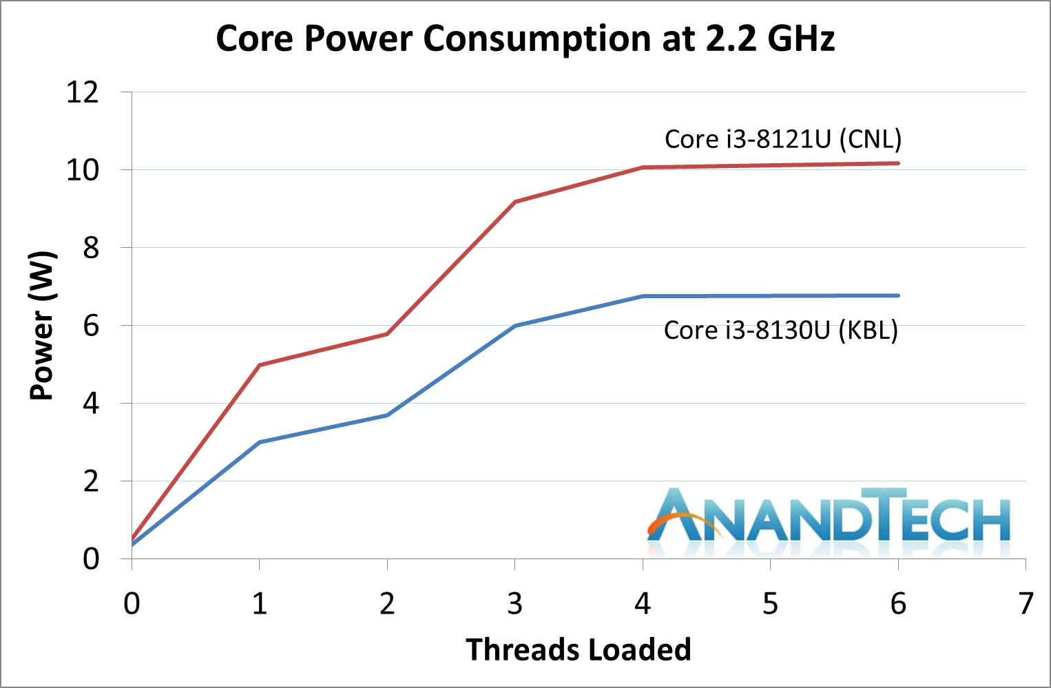
If this graph was the definitive graph, it shows that Cannon Lake is vastly inefficient (at 2.2 GHz) compared to Kaby Lake.


129 Comments
View All Comments
jjj - Friday, January 25, 2019 - link
Bored with laptops, want a large foldable phone with a projected keyboard so i can forget about these bulky heavy things. Ok, fair enough, glasses are way better but those will take a while longer.eastcoast_pete - Friday, January 25, 2019 - link
@Ian: Thanks for the deep dive, and giving the references for background! One comment, three questions (they're related): In addition to being very (overly) ambitious with the 10 nm process, I was particularly struck by the "fused-off integrated graphics" and how Intel's current 10 nm process apparently just won't play nice with the demands in a GPU setting. Question: Any information or rumors on whether that contributed to AMD going the chiplet route for Ryzen going forward? In addition to improving yields, that also allows for heterogeneous manufacturing nodes on the same final chip, so that can get around that problem. Finally, any signs that Intel may go down that road in its upcoming mainstream chips? Any updates on what node they will make their much-announced dGPUs on? Probably won't be this or a related 10 nm process.Lastly, and maybe you and Andrei can weigh in on that: TSMC's (different) 7 nm process seems to work okay for the (smaller) different "iGPUs" in Apple's 12/12x, Huawei's newest Kirin and the new Snapdragon. Any insight/speculation which steps of Intel's 10 nm process cause the apparent incompatibility with GPU usage scenarios?
Thanks!
Rudde - Saturday, January 26, 2019 - link
AMD has lauched huge 7nm desktop graphics cards (2 server and Radeon VII). AMD does not seem to have any problems making gpus on TSMC 7nm.eastcoast_pete - Sunday, January 27, 2019 - link
That's why I asked about the apparent incompatibility of GPU-type dies with Intel's 10 nm process. Isn't it curious that this seems to be the Achilles heel of Intel's process? I wonder if their future chips with " iGPU" will use a chiplet-type approach, with the CPU parts in 10 nm, and the GPU in 14 nm++++ or however many + generations it'd be on. The other big question is what process their upcoming high-end dGPU will be in Unless, Intel let's TSMC make that for them, too.velanapontinha - Friday, January 25, 2019 - link
Every time I read Kaby G I'm instantly stormed by a Kenny G theme stuck in my head, and it ruins the rest of my day.Please stop.
skis4hire - Friday, January 25, 2019 - link
"Fast forward several months later, to May 2018, and we still had not heard anything from Intel."Anton covered their statement in April, where they indicated they weren't shipping volume 10nm until sometime in 2019, and that they would instead release another 14nm product, whiskey lake, in the interim.
https://www.anandtech.com/show/12693/intel-delays-...
Yorgos - Friday, January 25, 2019 - link
>AMD XXXXX (XM/XT, XXW)Thanks Ian for reminding us is every article, that we are reading a Purch media product, or a clueless editor.
Don't forget, 386 was o 0 core CPU.
No, it doesn't bother me as a reader, it bothers me as an engineer who designs and studies digital circuits. But hey you can't have it all, it's hard to find someone who is capable at running windows executables AND know his way in comp. arch..
Ryan Smith - Friday, January 25, 2019 - link
While I'm all for constructive feedback, I have to admit I'm not sure what we're meant to be taking from this.Could you please articulate in more detail what exactly is wrong with the article?
KateH - Saturday, January 26, 2019 - link
i interpreted it as,...
"I disagree with the distinction between 'modules' and 'cores' that is made when some journalistic endevours mention AMD's 'Construction' architecture microprocessors. I find the drawing of a line based on FPU counts inaccurate- disengenous even- given that historic microprocessors such as the renowned Intel 80386 did not feature an on-chip FPU at all, an omission that would under the definitions used by this journalist in this article cause the '386 to be described as having 'zero cores'. The philosophical exercise suggested by such a definition is, based upon my extensive experience in the industry of digital circuit design, repugnant to my sensibilities and in my opinion calls into question the journalistic integrity of this very publication!"
...
or something like that
(automatically translated from Internet Hooligan to American English, tap here to rate translation)
Ryan Smith - Saturday, January 26, 2019 - link
"tap here to rate translation"5/5 stars. Thank you!