Intel's 10nm Cannon Lake and Core i3-8121U Deep Dive Review
by Ian Cutress on January 25, 2019 10:30 AM ESTCPU Performance: Memory and Power
Memory
With the same memory setup as the standard Skylake-style core, without any other improvements, we should expect Cannon Lake to perform exactly similar. Here’s a recap of the memory configuration:
| Memory Comparison | ||
| Skylake Desktop | Cannon Lake | |
| L1-D Cache |
32 KiB/core 8-way |
32 KiB/core 8-way |
| L1-I Cache |
32 KiB/core 8-way |
32 KiB/core 8-way |
| L2 Cache |
256 KiB/core 4-way |
256 KiB/core 4-way |
| L3 Cache |
2 MiB/core 16-way |
2 MiB/core 16-way |
| L3 Cache Type | Inclusive | Inclusive |
For this test we put our Cannon Lake and Kaby Lake processors through our Memory Latency Checker test. Both systems had turbo modes disabled, forcing them to run at 2.2 GHz for parity and a direct microarchitecture comparison.
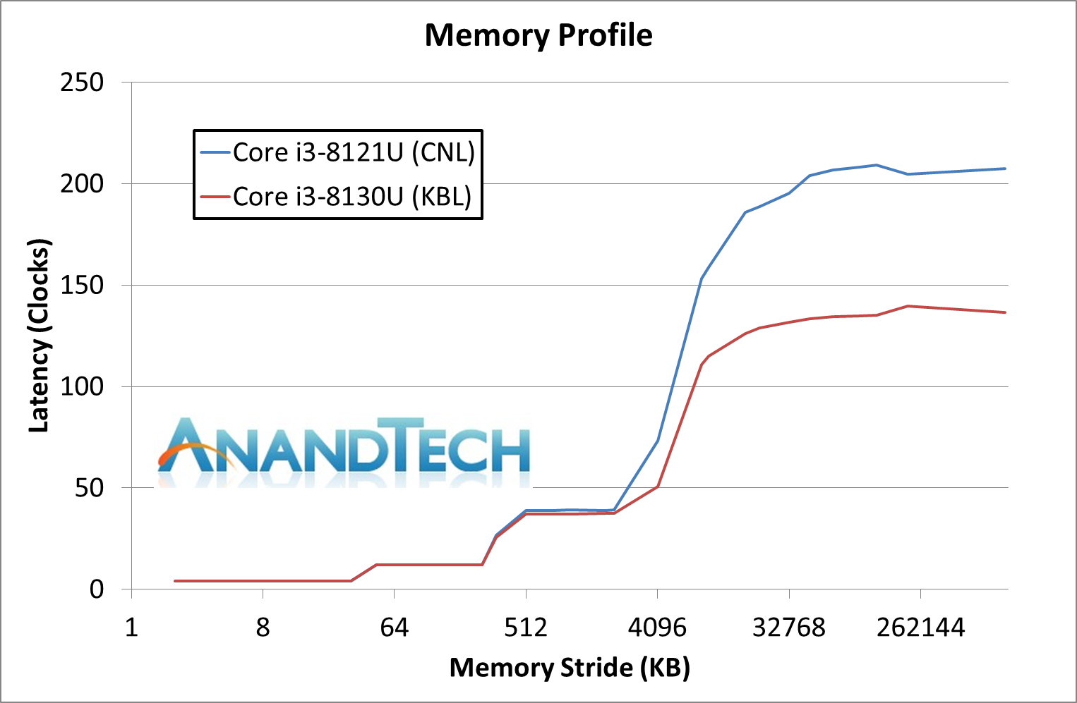
In this instance we see very little different between the two through the caches of the chip. Up to about 2MiB, both chips perform practically identical. Beyond this however, going out to main memory, there is a big discrepancy between the Kaby Lake and the Cannon Lake processor. In essence, accessing Cannon Lake main memory has an additional 50% latency.
At first we thought this was a bug. For both systems to have dual channel memory and running DDR4-2400, something had to be wrong. We double checked the setups – both systems were running in dual channel mode, giving the same memory bandwidth. The Cannon Lake processor was running at DDR4-2400 17-17-17, whereas the Kaby Lake system was at DDR4-2400 16-16-16 (due to memory SPD differences), which isn’t a big enough change to have such a big difference. The only reason we can come up with is that the memory controller on Cannon Lake must have additional overhead from the core to the memory controller – either a slower than expected PLL or something.
Power
Measuring the power of these thermally limited systems is somewhat frustrating in that we are at the whims of the quality of silicon at play. Bad silicon can get hotter faster, causing thermal throttling, or it depends on how the systems are set up for the peak power numbers. We use AIDA’s power monitoring tool to give us the power numbers for the CPUs during our POV-Ray test.
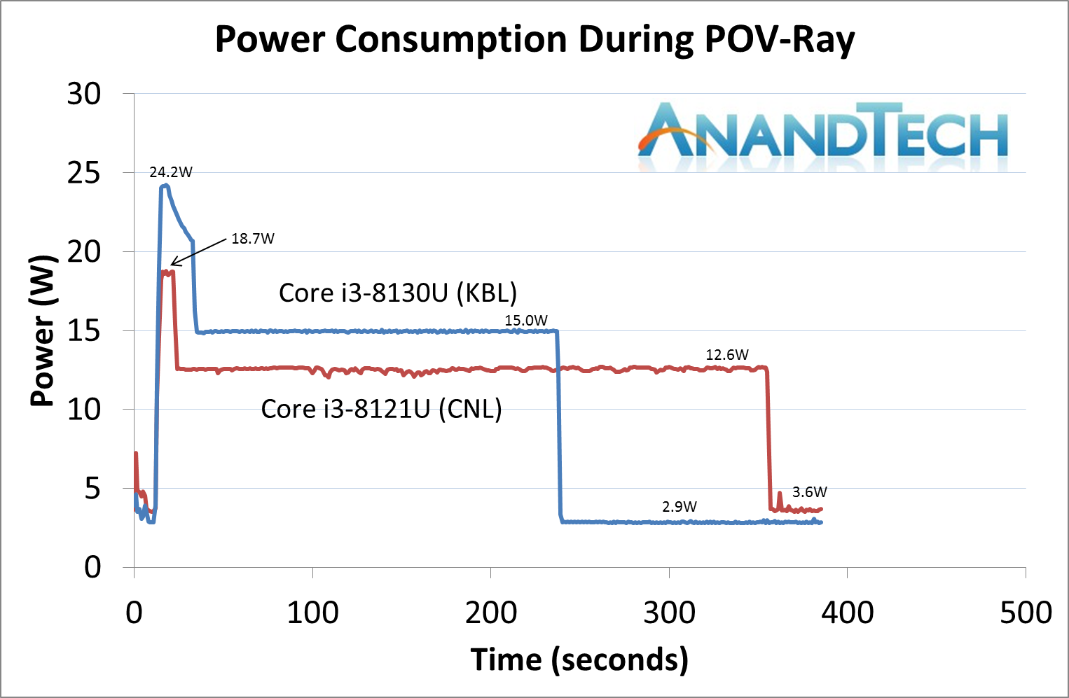
If you saw our How Intel Measures TDP article, you may be familiar with the concept of Power Limits. Intel processors have several power limits set in firmware – these values are set by the system manufacturer, and Intel provides ‘guidelines’. The two key values are Power Limit 1 (PL1), which describes a steady state scenario, and Power Limit 2 (PL2) which describes a turbo scenario. The reason why the system manufacturer gets control of these is because they might put a high wattage processor into a small form factor system, and need to manage performance – this is why we sometimes see a Core i7 be outperformed by a Core i5 in the same system design.
In most cases, PL1 is set to the TDP of the processor – in this case, it should be 15W. As shown on the graph above, this is true for our Core i3-8130U system, which shows a steady state power consumption of 15.0W. The Cannon Lake processor however only peaks at 12.6W.
PL2, the turbo power of the processor, can also be determined. For the Kaby Lake processor, we see a peak of 24.2 W, while the Cannon Lake has a turbo only of 18.7 W. We see that the turbo time period for the Cannon Lake processor is also much shorter, leading to a PL1 / steady state power much sooner.
Part of this is because we are pitting the Cannon Lake laptop against the Kaby Lake mini-PC. That being said, the Cannon Lake laptop is a beefy 15.6-inch unit, and has cooling for both the CPU and the discrete RX540 graphics, which isn’t doing much during this test except showing a basic 2D display.
That is arguably a lot more cooling than the mini-PC provides, plus we are cooling it with additional fans. These settings are more a function of both Lenovo doing what it wants to in firmware that we can’t change, but also the chip as engineered.
We can also calculate some level of efficiency here. By taking the area under the graph and correcting for the base line power (2.9 W on KBL, 3.6 W on CNL), we can calculate the total power consumed during the test. We get the following:
- Core i3-8121U (CNL) consumes 867 mWh
- Core i3-8130U (KBL) consumes 768 mWh
So this means that Cannon Lake is slower in AVX2 frequency, consumes more power, and scores 25% less in POV-Ray (see previous pages). That’s damning for the design.
To further look into this data, we disabled the turbo modes on both processors and ran our POV-Ray workload adjusting the number of threads being loaded and then measured the power consumption. In this scenario we are running at the same frequency, measuring the steady state power, and are thus at the whims of both the voltage set on both processors and the efficiency. Our tool also lets us measure the power of just the cores, so we’ll plot core power against threads loaded.
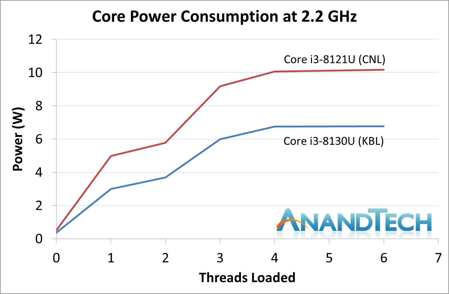
If this graph was the definitive graph, it shows that Cannon Lake is vastly inefficient (at 2.2 GHz) compared to Kaby Lake.


129 Comments
View All Comments
eva02langley - Sunday, January 27, 2019 - link
Even better...https://youtu.be/osSMJRyxG0k?t=1220
AntonErtl - Sunday, January 27, 2019 - link
Great Article! The title is a bit misleading given that it is much more than just a review. I found the historical perspective of the Intel processes most interesting: Other reporting often just reports on whatever comes out of the PR department of some company, and leaves the readers to compare for themselves with other reports; better reporting highlights some of the contradictions; but rarely do we se such a pervasive overview.The 8121U would be interesting to me to allow playing with AVX512, but the NUC is too expensive for me for that purpose, and I can wait until AMD or Intel provide it in a package with better value for money.
RamIt - Sunday, January 27, 2019 - link
Need gaming benches. This would make a great cs:s laptop for my daughter to game with me on.Byte - Monday, January 28, 2019 - link
Cannonlake, 2019's Broadwell.f4tali - Monday, January 28, 2019 - link
I can't believe I read this whole review from start to finish...And all the comments...
And let it sink in for over 24hrs...
But somehow my main takeaway is that 10nm is Intel's biggest graphics snafu yet.
(Well THAT and the fact you guys only have one Steam account!)
;)
NikosD - Monday, January 28, 2019 - link
@Ian CutressGreat article, it's going to become all-time classic and kudos for mentioning semiaccurate and Charlie for his work and inside information (and guts)
But really, how many days, weeks or even months did it take to finish it ?
bfonnes - Monday, January 28, 2019 - link
RIP IntelCharonPDX - Monday, January 28, 2019 - link
Insane to think that there have been as many 14nm "generations" as there were "Core architecture" generations before 14nm.ngazi - Tuesday, January 29, 2019 - link
Windows is snappy because there is no graphics switching. Any machine with the integrated graphics completely off is snappier.Catalina588 - Wednesday, January 30, 2019 - link
@Ian, This was a valuable article and it is clipped to Evernote. Thanks!Without becoming Seeking Alpha, you could add another dimension or two to the history and future of 10nm: cost per transistor and amortizing R&D costs. At Intel's November 2013 investor meeting, William Holt strongly argued that Intel would deliver the lowest cost per transistor (slide 13). Then-CFO Stacey Smith and other execs also touted this line for many quarters. But as your article points out, poor yields and added processing steps make 10nm a more expensive product than the 14nm++ we see today. How will that get sold and can Intel improve the margins over the life of 10nm?
Then there's amortizing the R&D costs. Intel has two independent design teams in Oregon and Israel. Each team in the good-old tick-tock days used to own a two-year process node and new microarchitecture. The costs for two teams over five-plus years without 10nm mainstream products yet is huge--likely hundreds of millions of dollars. My understanding is that Intel, under general accounting rules, has to write off the R&D expense over the useful life of the 10nm node, basically on a per chip basis. Did Intel start amortizing 10nm R&D with the "revenue" for Cannon Lake starting in 2017, or is all of the accrued R&D yet to hit the income statement? Wish I knew.
Anyway, it sure looks to me like we'll be looking back at 10nm in the mid-2020s as a ten-year lifecycle. A big comedown from a two-year TickTock cycle.