The NVIDIA Turing GPU Architecture Deep Dive: Prelude to GeForce RTX
by Nate Oh on September 14, 2018 12:30 PM ESTThe Turing Trio: TU102, TU104, & TU106
Altogether, NVIDIA will be kicking off the Turing generation with a trio of GPUs: TU102, TU104, and TU106. Notably, this is a much larger product stack than any past NVIDIA consumer launch. Typically NVIDIA releases just a single GPU on launch day – usually the 104 model – and then additional GPUs filter in months down the line as production ramps up. Instead NVIDIA will be releasing products based on two different GPUs this month, and then following that up with a third GPU one month later.
Since all three GPUs are Turing, all three GPUs share the same basic design, and in the same ratios. Meaning that TU104 and TU106 are proportionally cut-down versions of TU102, without any radical changes between the GPUs like we’ve seen between GP100 and GP102/104/106. This also means that TU104 and TU106 are proportionally powerful GPUs; NVIDIA hasn’t stripped TU106’s RT and tensor cores to a bare minimum to save on the transistor count, for example.
| NVIDIA Turing GPU Comparison | ||||||
| TU102 | TU104 | TU106 | GP102 | |||
| CUDA Cores | 4608 | 3072 | 2304 | 3840 | ||
| SMs | 72 | 48 | 36 | 30 | ||
| Texture Units | 288 | 192 | 144 | 240 | ||
| RT Cores | 72 | 48 | 36 | N/A | ||
| Tensor Cores | 576 | 384 | 288 | N/A | ||
| ROPs | 96 | 64 | 64 | 96 | ||
| Memory Bus Width | 384-bit | 256-bit | 256-bit | 384-bit | ||
| L2 Cache | 6MB | 4MB | 4MB | 3MB | ||
| Register File (Total) | 18MB | 12MB | 9MB | 7.5MB | ||
| Architecture | Turing | Turing | Turing | Pascal | ||
| Manufacturing Process | TSMC 12nm "FFN" | TSMC 12nm "FFN" | TSMC 12nm "FFN" | TSMC 16nm | ||
| Die Size | 754mm2 | 545mm2 | 445mm2 | 471mm2 | ||
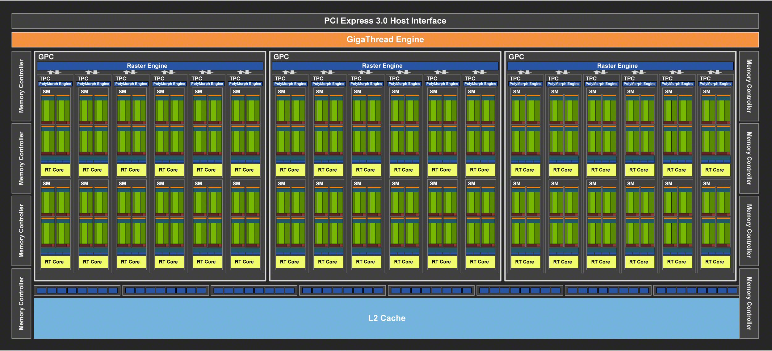
The flagship for the Turing family is a part that we’ve quickly become familiar with, and that is TU102. The largest of the Turing GPUs, this is the GPU NVIDIA is tapping for two of their new Quadro RTX cards, as well as the GeForce RTX 2080 Ti.
A fully-enabled TU102 is comprised of 72 SMs, organized into 6 GPCs. And since the number of RT cores and tensor cores is proportional to the SM count, we’re looking at 72 RT cores and 576 tensor cores. Paired with this harder is 12 ROP/memory controller partitions, giving the GPU a native 384-bit memory bus and 96 ROPs for pixel blending.
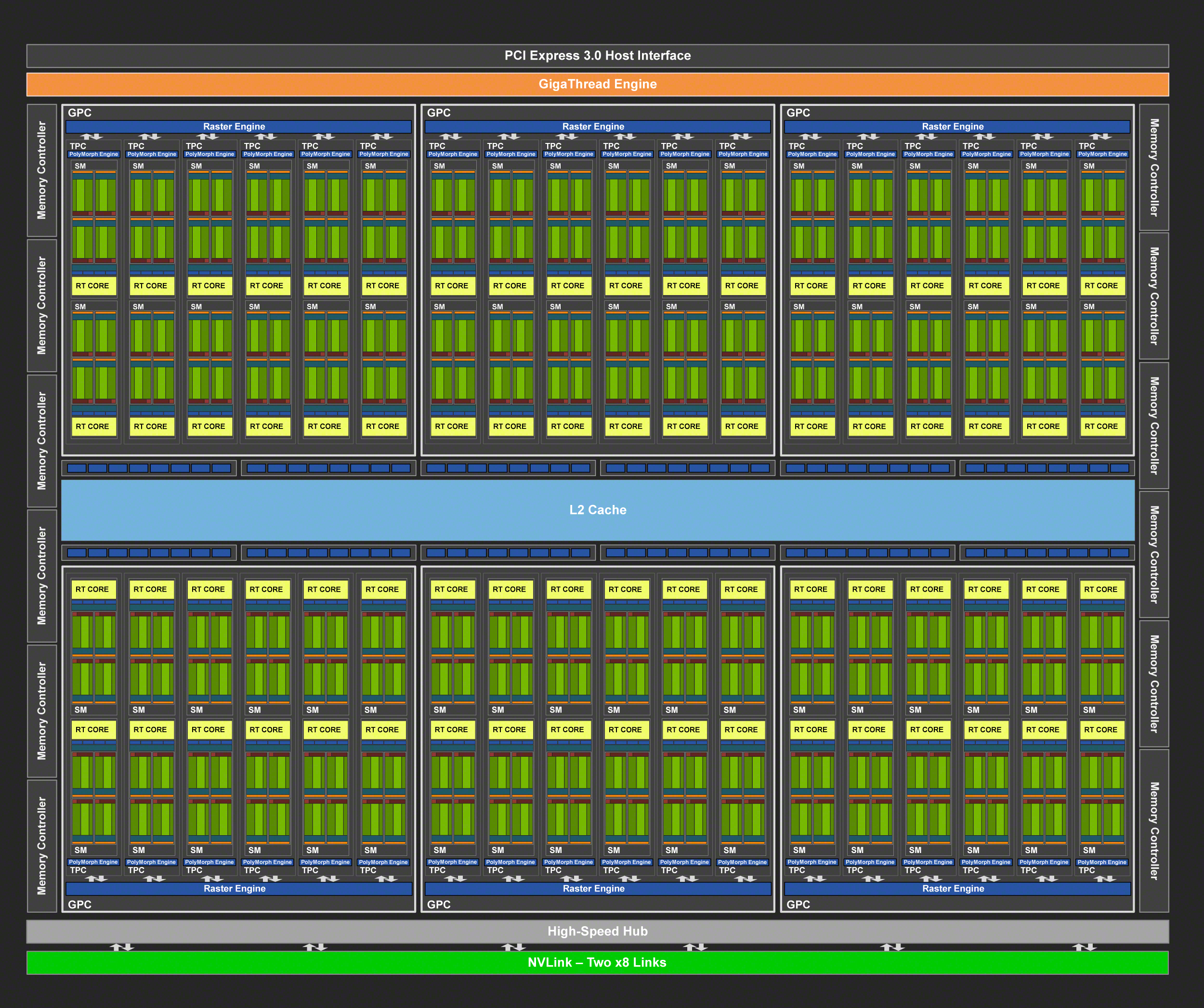
Relative to NVIDIA’s GV100 GPU, TU102 is smaller and contains fewer SM and tensor cores, but the difference is not quite as great as you might think. The 18.6B transistor, 754mm2 chip still packs 85% of GV100’s common hardware even with its physically small size, and then this value doesn’t include all the die space taking up by Turing’s new features such as the RT cores and the newer generation tensor cores. So this is still an incredibly big chip, and is especially notable since NVIDIA will be putting it in a consumer card.
Outside of the standard Turing graphics hardware, of particular note here is that because TU102 pulls double-duty with high-end Quadro cards, it’s the only GPU to feature two NVLink connections. Each NVLink connection – which NVIDIA technically classifies as an 8x NVlink – is capable of offering 25GB/sec of bandwidth in each direction, for a total of 50GB/sec of bandwidth in each direction when the links are used in aggregate.
The middle child of the stack and the traditional frontrunner in NVIDIA’s GPU release cadence is the TU104. This part is a smaller, slimmer Turing GPU that shaves off some SMs in the name of coming in at a smaller die size. Altogether it offers 48 SMs and 8 ROP/MC partitions, making it roughly two-thirds of a TP102.
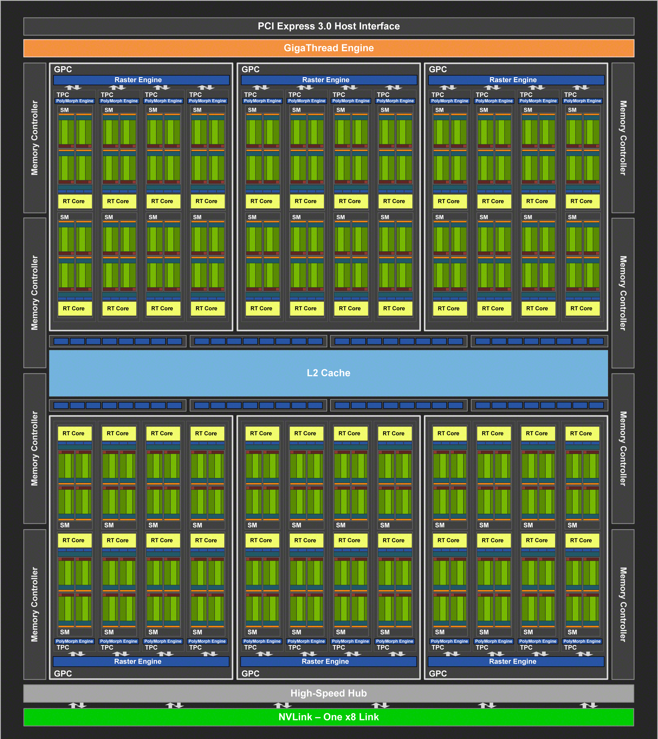
In exchange the chip is also notably smaller. Not small by any means, but smaller. The part comes in at 13.6B transistors, which are laid out in a 545mm2 die. This still makes it the largest x04 chip by a landslide, coming in much larger than even the late-generation 28nm GM204 in 2014. Still, NVIDIA shaved off over 200mm2 relative to TU102, so there are significant die savings here compared to using an actual cut-down TU102.
The TU104 will be going into just one consumer card, at least for now. This is the GeForce RTX 2080. It will also be going into its Quadro counterpart, the Quadro RTX 5000. Notably, only the Quadro is getting a fully enabled chip, while RTX 2080 ships with a couple of disabled SMs. This GPU also features NVLink support, but this time it’s a single x8 link, half of what TU102 offered.
Finally, rounding out the trio is the mysterious TU106 GPU, which prior to today had not been disclosed by NVIDIA. Rather than using a cut-down TU104 in the GeForce RTX 2070, they’re going to use an entirely different GPU.
TU106 in turn is a smaller chip than TU104, but perhaps not as much as you think. NVIDIA is still including 36 SMs and the same 8 ROP/MC partitions, so in terms of pixel throughput and bandwidth TU106 is actually identical to TU104 on paper. It’s only when looking at the processor elements that we see that we’ve ended up with what’s essentially 75% of a TU104. On which note however, it’s rather interesting that NVIDIA opted to halve the GPC count here; TU106 packs 12 SMs to a GPC, versus 8 to a GPC in TU104.
The payoff for NVIDIA here is that TU106 once again brings down NVIDIA’s large die sizes. The chip features 10.8 billion transistors, which at 445mm2 still makes it a beefy chip. But this is at least finally smaller than the GP102 used in the Pascal Titan Xp cards.
The net result of all of this is that NVIDIA has a very interesting GPU launch stack, one unlike anything we’ve seen before. No two GeForce cards share the same GPU; there is a GPU for each and every card right now. And we’re seeing NVIDIA launch two GPUs right out the door, including the massive TU102, with the TU106 to follow close behind. So it’s a very different setup than the norm for NVIDIA.
Turing In Practice: GeForce RTX 2080 Ti, 2080, & 2070
These 3 GPUs, in turn, form the foundation of the GeForce RTX 2080 Ti, RTX 2080, and RTX 2070. As previously announced by NVIDIA, the first two cards will go on sale next week, on September 20th. Meanwhile the RTX 2070 will ship a bit later, with sales starting in October.
We’ll be giving the RTX 2080 Ti and RTX 2080 a full work-through next week in our review of those cards. In the meantime, here’s a recap of their specifications and pricing.
| NVIDIA GeForce x80 Ti Specification Comparison | ||||||
| RTX 2080 Ti Founder's Edition |
RTX 2080 Ti | GTX 1080 Ti | GTX 980 Ti | |||
| CUDA Cores | 4352 | 4352 | 3584 | 2816 | ||
| ROPs | 88 | 88 | 88 | 96 | ||
| Core Clock | 1350MHz | 1350MHz | 1481MHz | 1000MHz | ||
| Boost Clock | 1635MHz | 1545MHz | 1582MHz | 1075MHz | ||
| Memory Clock | 14Gbps GDDR6 | 14Gbps GDDR6 | 11Gbps GDDR5X | 7Gbps GDDR5 | ||
| Memory Bus Width | 352-bit | 352-bit | 352-bit | 384-bit | ||
| VRAM | 11GB | 11GB | 11GB | 6GB | ||
| Single Precision Perf. | 14.2 TFLOPs | 13.4 TFLOPs | 11.3 TFLOPs | 6.1 TFLOPs | ||
| "RTX-OPS" | 78T | 78T | N/A | N/A | ||
| TDP | 260W | 250W | 250W | 250W | ||
| GPU | TU102 | TU102 | GP102 | GM200 | ||
| Architecture | Turing | Turing | Pascal | Maxwell | ||
| Manufacturing Process | TSMC 12nm "FFN" | TSMC 12nm "FFN" | TSMC 16nm | TSMC 28nm | ||
| Launch Date | 09/20/2018 | 09/20/2018 | 03/10/2017 | 06/01/2015 | ||
| Launch Price | $1199 | $999 | MSRP: $699 Founders: $699 |
$649 | ||
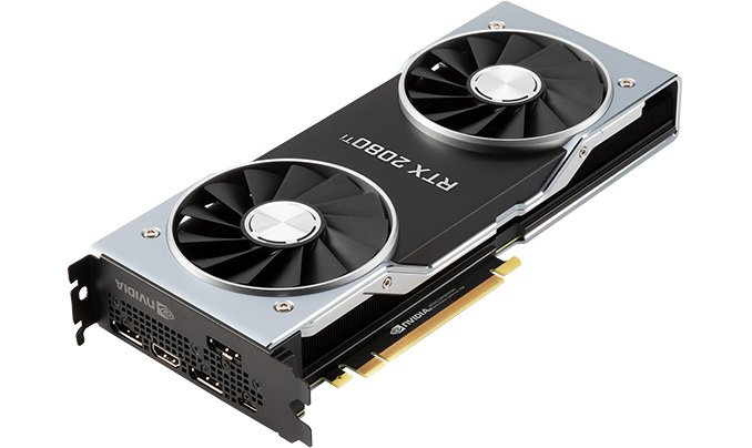
The king of NVIDIA’s new product stack, the GeForce RTX 2080 Ti is without a doubt an interesting card. NVIDIA’s consumer flagship sports 4352 Turing CUDA cores and 544 tensor cores, as well as 68 RT cores. Like its Quadro counterpart, this card is rated for 10 GigaRays/second, and for traditional compute we’re looking at 13.4 TFLOPS based on these specifications. Note that on paper this is only 19% higher than GTX 1080 Ti, which is why NVIDIA’s architectural changes and efficiency improvements are going to carry the day here, rather than brute forcing the matter with more hardware.
Clockspeeds have actually dropped from generation to generation here. Whereas the GTX 1080 Ti started at 1.48GHz and had an official boost clock rating of 1.58GHz (and in practice boosting higher still), RTX 2080 Ti starts at 1.35GHz and boosts to 1.55GHz, while we don’t know anything about the practical boost limits. So assuming NVIDIA is being as equally conservative as the last generation, then this means the average clockspeeds have dropped slightly.
Moving on, for the ROP and memory subsystem we’re looking at a partially-enabled configuration here as well. RTX 2080 Ti offers 88 of 96 ROPs, which is a result of NVIDIA disabling one of the 12 ROP/MC partitions. Even then, relative to the GTX 1080 Ti and thanks to GDDR6, memory clockspeeds have been boosted from 11Gbps to 14Gbps, a 27% increase. And since the memory bus width itself remains identical at 352-bits wide, this means the final memory bandwidth increase is also 27%.
Past this, things start diverging a bit. NVIDIA is once again offering their reference-grade Founders Edition cards, and unlike with the GeForce 10 series, the 20 series FE cards have slightly different specifications than their base specification compatriots. Specifically, NVIDIA has cranked up the clockspeed and the resulting TDP a bit, giving the 2080 Ti FE an on-paper 6% performance advantage, and also a 10W higher TDP. For the standard cards then, the TDP is the x80 Ti-traditional 250W, while the FE card moves to 260W.
| NVIDIA GeForce x80 Specification Comparison | ||||||
| RTX 2080 Founder's Edition |
RTX 2080 | GTX 1080 | GTX 980 | |||
| CUDA Cores | 2944 | 2944 | 2560 | 2048 | ||
| ROPs | 64 | 64 | 64 | 64 | ||
| Core Clock | 1515MHz | 1515MHz | 1607MHz | 1126MHz | ||
| Boost Clock | 1800MHz | 1710MHz | 1733MHz | 1216MHz | ||
| Memory Clock | 14Gbps GDDR6 | 14Gbps GDDR6 | 10Gbps GDDR5X | 7Gbps GDDR5 | ||
| Memory Bus Width | 256-bit | 256-bit | 256-bit | 256-bit | ||
| VRAM | 8GB | 8GB | 8GB | 4GB | ||
| Single Precision Perf. | 10.6 TFLOPs | 10.1 TFLOPs | 8.9 TFLOPs | 5.0 TFLOPs | ||
| "RTX-OPS" | 60T | 60T | N/A | N/A | ||
| TDP | 225W | 215W | 180W | 165W | ||
| GPU | TU104 | TU104 | GP104 | GM204 | ||
| Architecture | Turing | Turing | Pascal | Maxwell | ||
| Manufacturing Process | TSMC 12nm "FFN" | TSMC 12nm "FFN" | TSMC 16nm | TSMC 28nm | ||
| Launch Date | 09/20/2018 | 09/20/2018 | 05/27/2016 | 09/18/2014 | ||
| Launch Price | $799 | $699 | MSRP: $599 Founders $699 |
$549 | ||
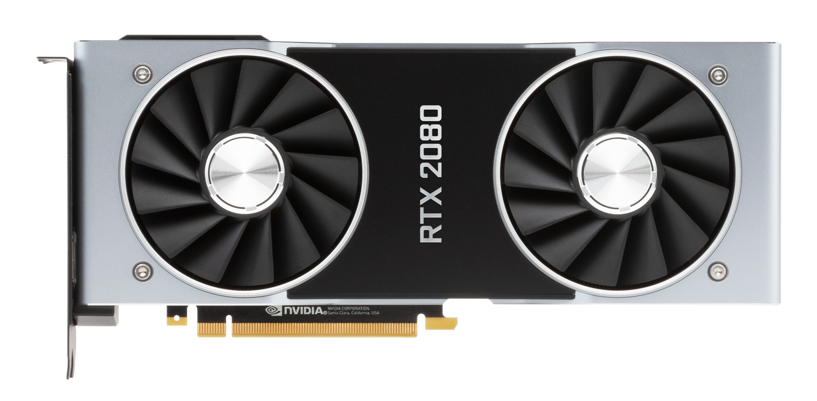
Moving down the line, we have the GeForce RTX 2080. Based on TU104, this card offers 2944 CUDA cores paired with 368 tensor cores. Like the RTX 1080 Ti, clockspeeds have dropped a bit from generation to generation, as the base clock is down to 1515MHz and the boost clock to 1710MHz. All told we’re looking at a pure CUDA core compute throughput of 10.1 TFLOPs, about 13% higher than the GTX 1080. Or if we compare it to the RTX 2080 Ti, we’d see around 75% of the expected compute/tensor performance, which is only a bit larger than the jump we saw between the GTX 1080 and GTX 1080 Ti.
Meanwhile the card does come with a fully enabled memory bus, meaning we’re looking at 8GB of GDDR6 running at 14Gbps, on top of a 256-bit memory bus. Relative to the GTX 1080 this is an even more significant 40% increase in memory bandwidth.
As for TDPs, they’ve gone up for this band of cards. The stock RTX 2080 will have a 215W TDP, up 30W from the GTX 1080’s 180W TDP, and an even bigger increase if we look at GTX 980’s 165W TDP. It’s no secret that NVIDIA is fighting a losing battle with Moore’s Law here, and barring massive efficiency improvements, there is a need to increase TDPs to keep up overall performance. TU104 is a big chip, and without a full node shrink, it would seem that NVIDIA has to pay a power penalty instead. In the meantime this higher TDP also negates some of the RTX 2080 Ti’s power disadvantage, as now that gap is just 35W instead of 65W.
| NVIDIA GeForce x70 Specification Comparison | ||||||
| RTX 2070 Founder's Edition |
RTX 2070 | GTX 1070 | GTX 970 | |||
| CUDA Cores | 2304 | 2304 | 1920 | 1664 | ||
| ROPs | 64 | 64 | 64 | 64 | ||
| Core Clock | 1410MHz | 1410MHz | 1506MHz | 1050MHz | ||
| Boost Clock | 1710MHz | 1620MHz | 1683MHz | 1178MHz | ||
| Memory Clock | 14Gbps GDDR6 | 14Gbps GDDR6 | 8Gbps GDDR5 | 7Gbps GDDR5 | ||
| Memory Bus Width | 256-bit | 256-bit | 256-bit | 256-bit | ||
| VRAM | 8GB | 8GB | 8GB | 4GB | ||
| Single Precision Perf. | 7.9 TFLOPs | 7.5 TFLOPs | 6.5 TFLOPs | 3.9 TFLOPs | ||
| "RTX-OPS" | 45T | 45T | N/A | N/A | ||
| TDP | 185W | 175W | 150W | 145W | ||
| GPU | TU106 | TU106 | GP104 | GM204 | ||
| Architecture | Turing | Turing | Pascal | Maxwell | ||
| Manufacturing Process | TSMC 12nm "FFN" | TSMC 12nm "FFN" | TSMC 16nm | TSMC 28nm | ||
| Launch Date | 09/20/2018 | 09/20/2018 | 06/10/2016 | 09/18/2014 | ||
| Launch Price | $599 | $499 | MSRP: $379 Founders $449 |
$329 | ||
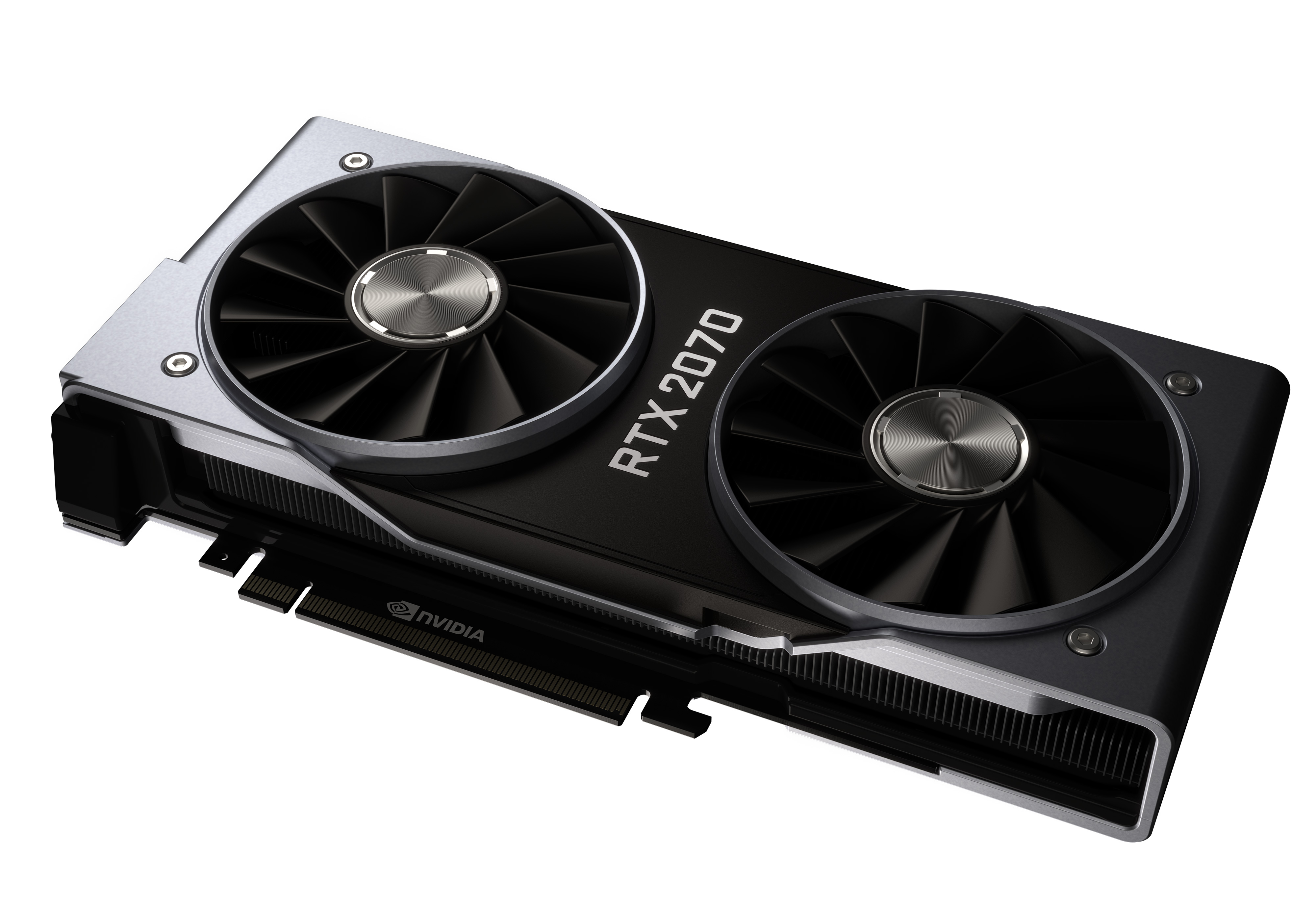
The final member of the new GeForce RTX family is the GeForce RTX 2070. Traditional for its roots, this is the “value” enthusiast card, giving up some of the RTX 2080’s performance in exchange for a lower price. Though with prices starting at $499, “value” and “cheap” are not the same thing.
With TU106, NVIDIA has shaved off a number of SMs. The end result is that the RTX 2070 offers 2304 CUDA cores and 288 tensor cores. Meanwhile ray tracing performance is rated at 6 GigaRays/second. Meanwhile in an interesting twist, this is the only consumer part launching with a fully-enabled GPU: TU106 offers 36 SMs, and NVIDIA is using all 36 of them.
Like the other RTX cards, clockspeeds have dropped a bit versus the previous generation; the base clock now starts at 1410MHz, and the boost clock is 1620MHz. On paper then, compute throughput works out to 7.5 TFLOPs, up 15% from GTX 1070. Or if we compare it to the 2080, the 2070 should deliver around 75% of its bigger sibling’s compute performance, which makes the jumps between the 2070, 2080, and 2080 Ti all very symmetrical. This is also an ever so slightly smaller gap than what was between the GTX 1080 and GTX 1070.
Also like the RTX 2080, this appears to be a fully enabled memory configuration. Meaning we’re looking at 8GB of GDDR6 running at 14Gbps, on top of a 256-bit memory bus. Relative to the GTX 1070 this is the single greatest bandwidth increase of all of the RTX cards; the 2070 will enjoy a 75% increase in memory bandwidth over its Pascal predecessor, as the GTX 1070 never did use GDDR5X.
TDPs have gone up here as well. The RTX 2070 is rated for 175W, up from 150W for the GTX 1070, and 145W for the GTX 970. As with the RTX 2080, it looks like NVIDIA is paying for their performance and new features via higher power consumption in lieu of a full node shrink.


111 Comments
View All Comments
bernstein - Friday, September 14, 2018 - link
a lot of this will also depend on what kind of silicon ends up in the next playstation & xbox generation...Spunjji - Monday, September 17, 2018 - link
Isn't that already pretty much pinned to AMD? AFAIK Navi is pretty much the consumer interpretation of AMD's PS5 design. Microsoft really aren't likely to jump ship because of their history with Nvidia.Yojimbo - Saturday, September 15, 2018 - link
I think Turing's price/perf ratio will be better than Pascal's. It's the increase in price/performance that is not spectacular. But since AMD isn't releasing anything at all, that doesn't reflect negatively on Turing in any way.I don't know why people are throwing around this "50% of transistors" idea. Where is this information coming from?
Of course Turing will be crushed by a next generation of 7 nm GPUs that is architected equally as well, as such GPUs will have both additional time for architectural improvements and the advantage of a full node shrink. That will be true for both hybrid and raster-only rendering. And it would have been true for raster rendering no matter if RT cores were included or not.
It sounds like NVIDIA is providing the DLSS service to developers for free. I'd expect DLSS usage to be widespread for any developers interested in making games geared towards the 4K market.
I am guessing that Microsoft, at least, will want a raytracing-capable GPU in its next console. I doubt they would spend the effort to make the DXR API extension and then leave the technology out of their console, especially considering the convergence of console and PC gaming they seem to be pushing for.
jwcalla - Friday, September 14, 2018 - link
This is probably my first disinterested nvidia launch. Tensor cores and ray tracing don't really get me excited. I can't imagine half a die used for that stuff. Do the graphics really look that much better? Does hyper-realism even matter?Dizoja86 - Friday, September 14, 2018 - link
It doesn't even have to be hyper-realism. Just the basic limitations you can see with rasterized reflections in the Battlefield V tech demo paints a strong case for the use of ray-tracing. Being able to see reflections of objects that aren't directly on the screen in front of you seems like an important thing to move towards.HollyDOL - Saturday, September 15, 2018 - link
classic rasterized shading and reflection is basically one big cheat on human eye. Imagine something along mp3 128kbit being 'cd quality'. Trying to get that cheat closer and closer to 'reality' is more and more a challenge and resource eater. Ray-Tracing _should_ be able to quite simplify the issue on development front in future. And that's not considering possible visuals quality raise.Tamz_msc - Saturday, September 15, 2018 - link
Lol, players are complaining that in BF V it is hard to distinguish between friendlies and enemies. Adding RTX reflections to the mix would just make it worse.jwcalla - Saturday, September 15, 2018 - link
Watching the Battlefield tech demo (and the others), I didn't think it added a lot of value. When you analyze it side-by-side with a magnifying glass, yes, you can see some differences. I just don't think they're that dramatic and in the heat of game play you're not even going to recognize it. The improvements to global illumination look good though.I just feel like the industry has lost a lot of focus.
RSAUser - Saturday, September 15, 2018 - link
In a game like BF V, you're not just going to stand there looking at reflections, and it's going to hammer your frame rate/force you to go to 1080p or lower.I'd rather turn it off and have a high fps on 4k, tyvm, same as near everyone turned off hairworks for witcher 3, though with that it was at least single player so you'd sacrifice performance for visuals.
Dizoja86 - Friday, September 14, 2018 - link
Sometimes I get frustrated with Anandtech, but being able to have these fantastic articles when new technology is released is why I keep coming back.