Synopsys Demonstrates CXL and CCIX 1.1 over PCIe 5.0: Next-Gen In Action
by Anton Shilov on October 11, 2019 10:00 AM EST- Posted in
- Interconnect
- CCIX
- Synopsys
- CXL
Synopsys, one of the leading developers of chip development tools and silicon IP, demonstrated its CXL over PCIe 5.0 as well as CCIX 1.1 over PCIe 5.0 solutions at ArmTechCon 2019. The showcase indicates that the company’s IP is up and running, and is ready to be licensed by interested parties.
CXL and CCIX are chip-to-chip interconnect protocols for connecting processors to various accelerators that maintains memory and cache coherency at low latencies. Both protocols are designed for heterogeneous systems that use traditional CPUs along with accelerators featuring scalar, vector, matrix, and spatial architectures. Both CXL 1.0/1.1 as well as CCIX 1.1 use PCIe Gen 5 PHY stack at 32 GT/s per lane and support different link width natively. Aiming the same market segment and using the same physical interface, the CXL and CCIX protocols have numerous differences both on hardware as well as firmware/software side of things and will therefore compete against each other. Meanwhile, providers of silicon IP are gearing up to support both CXL and CCIX as they have a broad range of customers.
Synopsys recently introduced its 16-lane DesignWare CXL IP solution for SoCs to be made using 16 nm, 10 nm, and 7 nm FinFET process technologies. The package comprises the company’s CXL 1.1-compliant controller (supporting CXL.io, CXL.cache, CXL.mem protocols), silicon-proven PCIe Gen 5 controller, silicon-proven 32 GT/s PHY (allowing >36 dB channel loss across power, voltage, and temperature variations for long reach connections), RAS capabilities, and VC Verification IP.

The company yet has to formally announce availability of its DesignWare CCIX 1.1 IP package that will enable implementation of a CCIX 1.1 over PCIe Gen 5 at 32 GT/s speed, but at ArmTechCon the company demonstrated that the solution is already functional.
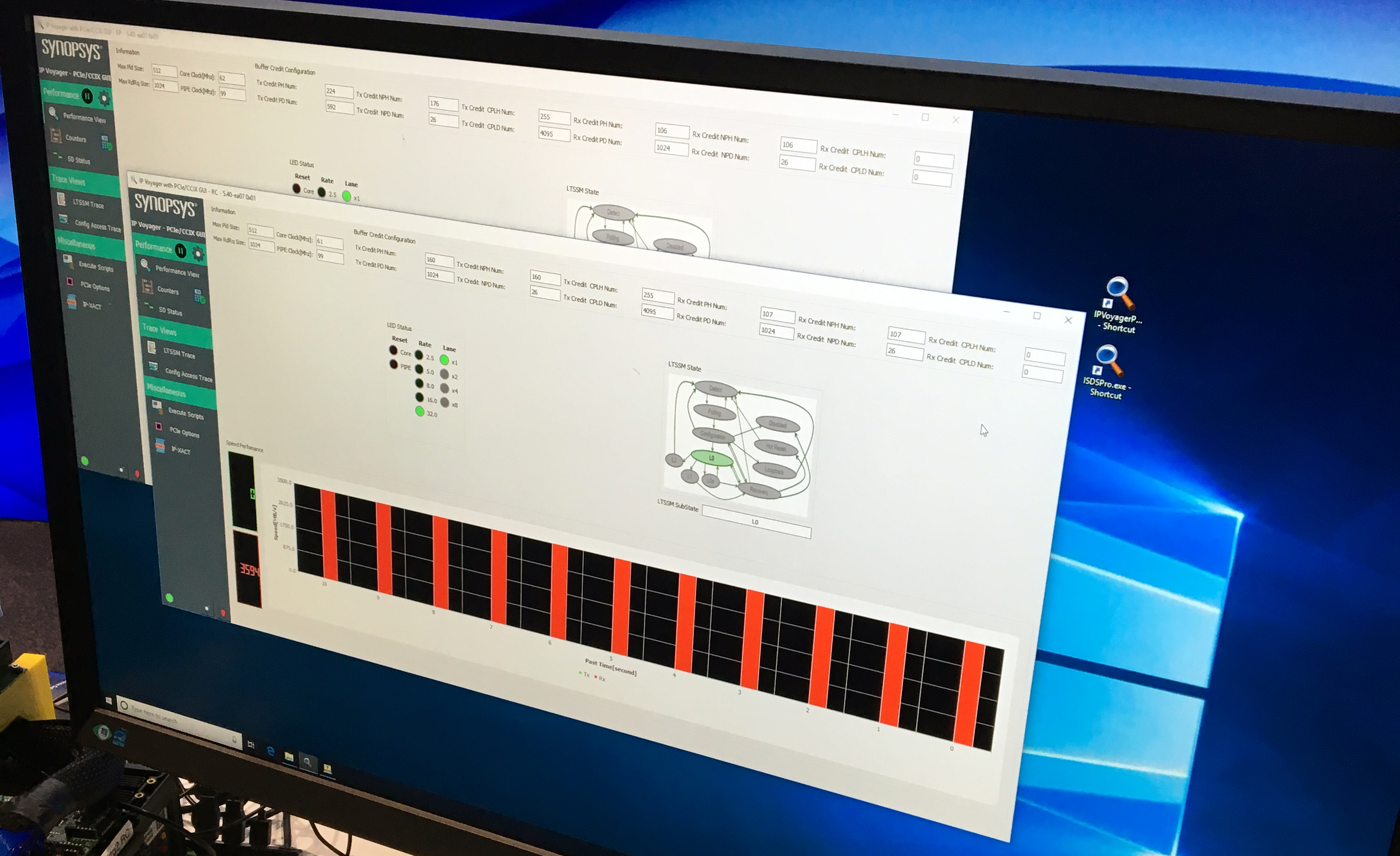
Both showcases were carried out using an FPGA as well as special equipment, but not using actual chips, which is not particularly surprising. But even such demonstrations indicate that Synopsys is ready not only with competitive PCIe 5.0 PHY and IP, but also with CXL and CCIX implementations.
Related Reading:
- Gen-Z PHY Specification 1.1 Published: Adds PCIe 5.0, Gen-Z 50G Fabric
- PCI-SIG Finalizes PCIe 5.0 Specification: x16 Slots to Reach 64GB/sec
- USB 3.2 at 20 Gb/s Coming to High-End Desktops This Year
Sources: David Schor/Twitter, Anshel Sag/Twitter, Synopsys
Images by Ryan Smith/AnandTech


4 Comments
View All Comments
alpha754293 - Friday, October 11, 2019 - link
This works well for core-to-core (or socket-to-socket) communications (let alone node-to-node), but eventually, it'll run into the biggest problem with HPC -- storage.Santoval - Saturday, October 12, 2019 - link
"Eventually", when storage becomes the bottleneck, non volatile memory could be used to replace NAND based SSDs, just as they are in the (long) process of replacing mechanical hard disks for almost all tasks except cold storage. Intel & Micron's 3D XPoint was a good start, but it's not as fast as (STT-)MRAM, for instance, which is faster even than DRAM and almost as fast as 6T-SRAM (still only at small sizes / low densities, unfortunately; MRAM starts to lose speed quickly at higher densities).Diogene7 - Saturday, October 12, 2019 - link
@Santoval : I agree with your view : there is a huge need for different low latency (less than 100ns) Non Volatile Memory (NVM) with a high enough density (probably at least GB) !!!Regarding MRAM, there seems to be many different version of MRAM like STT-MRAM and SOT-MRAM.
I read some a (research) articles about work done by the Begium micro-electronic research center, IMEC about STT-MRAM / SOT-MRAM
My understanding is that STT-MRAM seems to have an access latency between approx. 1ns and 10ns, and SOT-MRAM access latency between approx 0.1ns and 1ns
Therefore the faster SOT-MRAM seems to be considered for L1 / L2 (and I would think L3) cache replacement, and STT-MRAM could be fit for L3 cache replacement / DRAM but seems not fast enough for L1/L2 cache.
Also it seems that IMEC has shown that a STT-MRAM (L3) cache seems to take less physical space that a SRAM cache at 5nm.
As of 2019, however, STT-MRAM is a more « mature » technology, and virtually all the biggest foundries (TSMC, Samsung, Globalfoundries) and also Intel seems to be working to introduce it in High Volume Manufacturing : so I have my fingers crossed that some innovative 5nm or below mobile SoC will apear on the market between H2 2020 (Apple A14 ?) and let say H2 2023 at latest : the sooner, the better as low latency NVM is key for real improvement to reduce / eliminate the painful latency of boot time / load time !!!
Diogene7 - Friday, October 11, 2019 - link
@Anton Shilov: My undestanding is that CXL / CCIX protocols are, at the moment, more intended for data-centers scenarii.But, in theory, could it be possible to implement tje CXL (and also Gen-Z) protocols in a mobile SoC like for a future Qualcomm Snapdragon 875 that should be realeased around December 2020 / Qualcomm Snapdragon 885 (December 2021) ?
The goal would be to have a powerfull « generic » mobile SoC, to which could be attach different kind of chiplet accelerator (through CXL) / Storage Class Memory (SCM) (through Gen-Z) to easierly create different kind of mobile devices with different specialization ?