HiSilicon Announces New Kirin 950 SoC
by Andrei Frumusanu on November 5, 2015 11:20 AM EST
Today in Beijing, HiSilicon held an extensive media briefing on their brand new flagship SoC - the Kirin 950. The new chipset is a very large leap for the Huawei subsidiary as it represents the first true flagship successor to the Kirin 920 that we've seen a little over a year ago in the Honor 6 review.
In the past our analysis of the Kirin chipset's overall performance in phones such as the Mate 7 or the new P8 was not overly positive. The reason to this was mostly due to lacklustre showing of the GPU and general low efficiency of the SoC. The new chipset, the Kirin 950, promises to bring a lot of improvements and also represents a lot of firsts for the company.
| HiSilicon High-End Kirin Lineup | |||
| SoC | Kirin 920/925 | Kirin 930/935 | Kirin 950 |
| CPU | 4x Cortex A15 (1.7/1.8 GHz) 4x Cortex A7 (1.3GHz) |
4x Cortex A53 (2.0/2.2 GHz) 4x Cortex A53 (1.5 GHz) |
4x Cortex A72 (2.3 GHz) 4x Cortex A53 (1.8 GHz) |
| Memory Controller |
2x 32-bit LPDDR3 @ 800MHz 12.8GB/s b/w |
2x 32-bit LPDDR3 or LPDDR4 (hybrid controller) |
|
| GPU | Mali T628MP4 600MHz |
Mali T628MP4 680MHz |
Mali T880MP4 900MHz |
| Encode/ Decode |
1080p H.264 Decode & Encode |
1080p H.264 Decode & Encode 2160p30 HEVC Decode |
|
| Camera/ISP | Bad One (Needs Improvement) | Dual 14bit ISP 940MP/s |
|
| Integrated Modem |
Balong Integrated UE Cat. 6 LTE |
||
In terms of CPU HiSilicon continues the usage of a traditional big.LITTLE setup with four Cortex A72 and four A53 cores. This effectively makes HiSilicon the second vendor after MediaTek to ship ARM's new CPU core and the first one to do so in a mobile device. Thanks to the new process node the big core's frequency is able to be pushed up to 2.3GHz while the little cores clock in at up to 1.8GHz. HiSilicon estimates that the A72 is overall 11% faster clock-for-clock than current A57 designs, so together with the slightly higher clocks we should see the Kirin 950 perform about 20% better than the Exynos 7420 in CPU-bound tasks.
On the GPU side, the Kirin 950 gets an upgrade to Mali's new T880 GPU, again making this the first silicon implementation of the new ARM IP. The designers chose to remain with an MP4 configuration, but with a vastly increased clock rate of to up to 900MHz. I asked the company's senior planning manager as to why they chose to go with a lower core count and high frequency over a potentially more power efficient wider implementation at lower clock speeds, and the answer seems to be strikingly similar to MediaTek's explanation to the same question:
For the very vast majority of use-cases and users the GPU isn't a bottleneck and the full potential of more powerful GPUs are never utilized, so the vendors prefer to save die space and thus cost by using less GPU cores. As such, while the upgrade represents a significant improvement over previous Kirin chipsets, one shouldn't expect it to compete with more powerful alternatives such as from Qualcomm or Samsung.
Due to the new SoC having both A72 CPU cores and the new T880 Mali GPU I was expecting it to also ship with ARM's new CCI-500 - after all, 3 IPs were launched simultaneously back in February. Unfortunately HiSilicon explained that the new interconnect wasn't ready during the Kirin 950's design phase and thus the designers had to rely on the older CCI-400 that has been used in all big.LITTLE SoCs released to date.
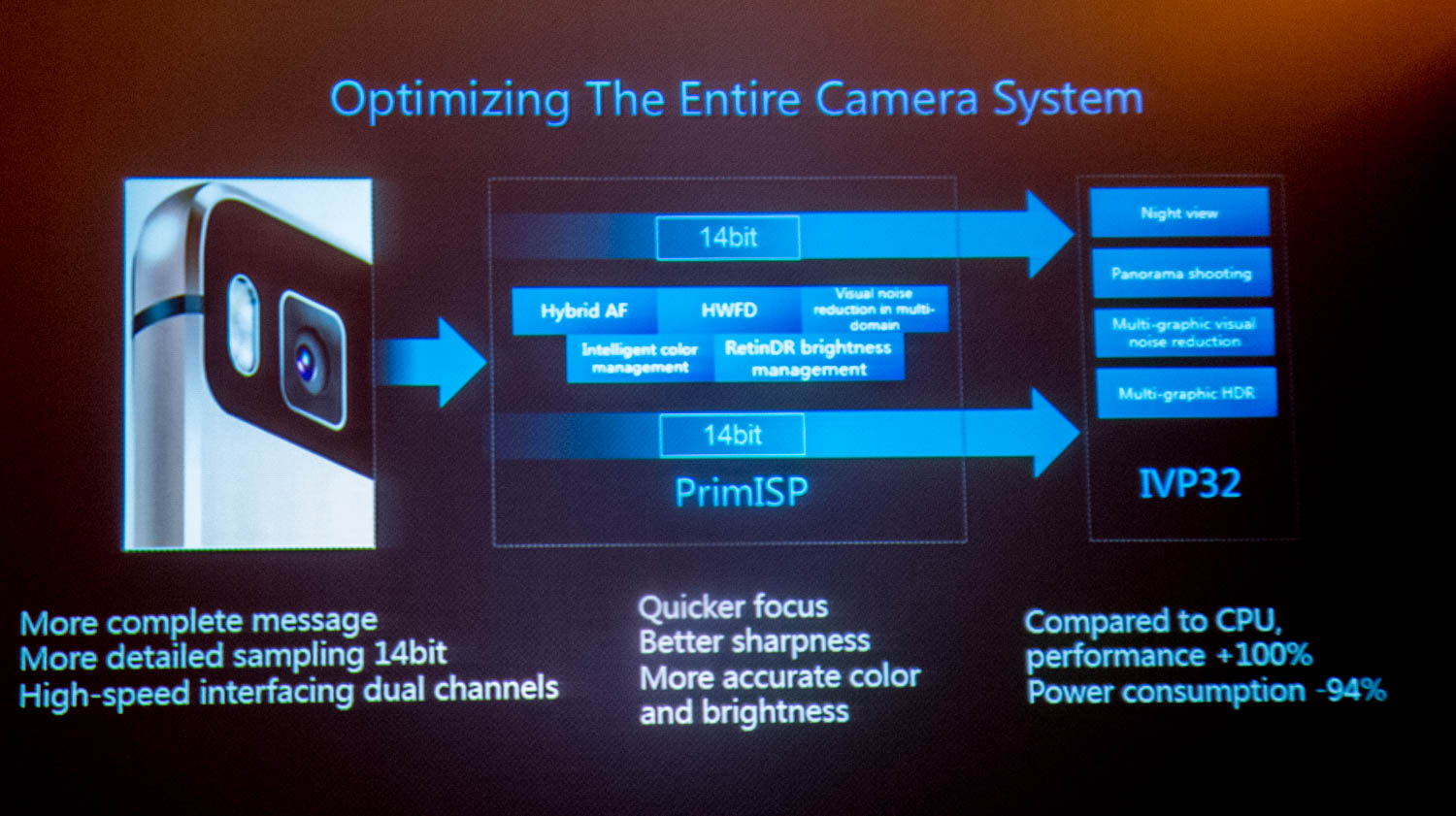
HiSilicon claims to have made some significant leaps in terms of ISP and DSP performance. In fact, the Kirin 950 is the first SoC that uses their newly developed PrimISP and IVP32 DSP. The new IP arose in part out of the 2013 recruitment of ex-Texas Instrument's OMAP SoC engineers in Nice, France. The subsequent founding of Huawei's Image Technology R&D Center allowed the company to have the design resources to build products tailored to their needs. As such, Huawei is finally able to sport a cutting-edge and competitive ISP/DSP integrated in the SoC which in the future will be able avoid usage of dedicated external ISP's such as those employed in this year's Huawei devices such as the Honor 6+, P8 or Mate S.
On the multimedia side, the company did not talk much about its encode and decode capabilities, limiting it to a single line in a single slide of their presentation, meaning we had to probe for further details. While the new SoC can now decode HEVC at up to 4K resolution at 30fps, the encode capabilities have not evolved from the previous generation and thus is limited to 1080p30 H.264. This also means that while the ISP would be able to handle 4K video, the actual encoder would make it impossible to actually implement 4K recording on a device product without a reduction in frame rate.
In terms of memory subsystem, the SoC is the first in the mobile industry to employ a hybrid LPDDR3 / LPDDR4 memory controller. It was only last week that ARM had announced a similar IP in the form of the DMC-500, but HiSilicon explained that the block employed in the Kirin 950 is of their own design and they were very proud to be able to offer this capability ahead of the competition.
In terms of connectivity, the SoC still employs an integrated Balong modem capable of 5-mode UE Category 6 LTE speeds of up to 300 Mbps. There wasn't much talk about the modem so likely the improvements were kept relatively minor.
Lastly, we saw an upgrade to the SoC's sensor-hub. The new i5 succeeds the i3 used in the Kirin 92X and 930s. The new co-processor is powered by an ARM Cortex M7 core which is able to provide much more processing performance at much lower power, including an FP unit and other controls.
TSMC 16FF+ Manufactured
As mentioned earlier, the Kirin 950 is HiSilicon's first TSMC 16FF+ manufactured mobile SoC. This also makes the Chinese vendor second in line after Apple's to release mobile silicon based on the new manufacturing node.
In fact, HiSilicon explains that along with Apple they've been the two main lead partners of the Taiwanese semiconductor giant, and both parties have been working closely together to try to improve the design and to tune the process. In fact, the company revealed that first mass production (also commonly named as risk production) started as early as last January. Over the following months both companies cooperated to sort out bugs and imperfections in the design (chip revisions) to go up from 20% yield in the earliest runs to up to 80% yields and qualified mass production this last August.
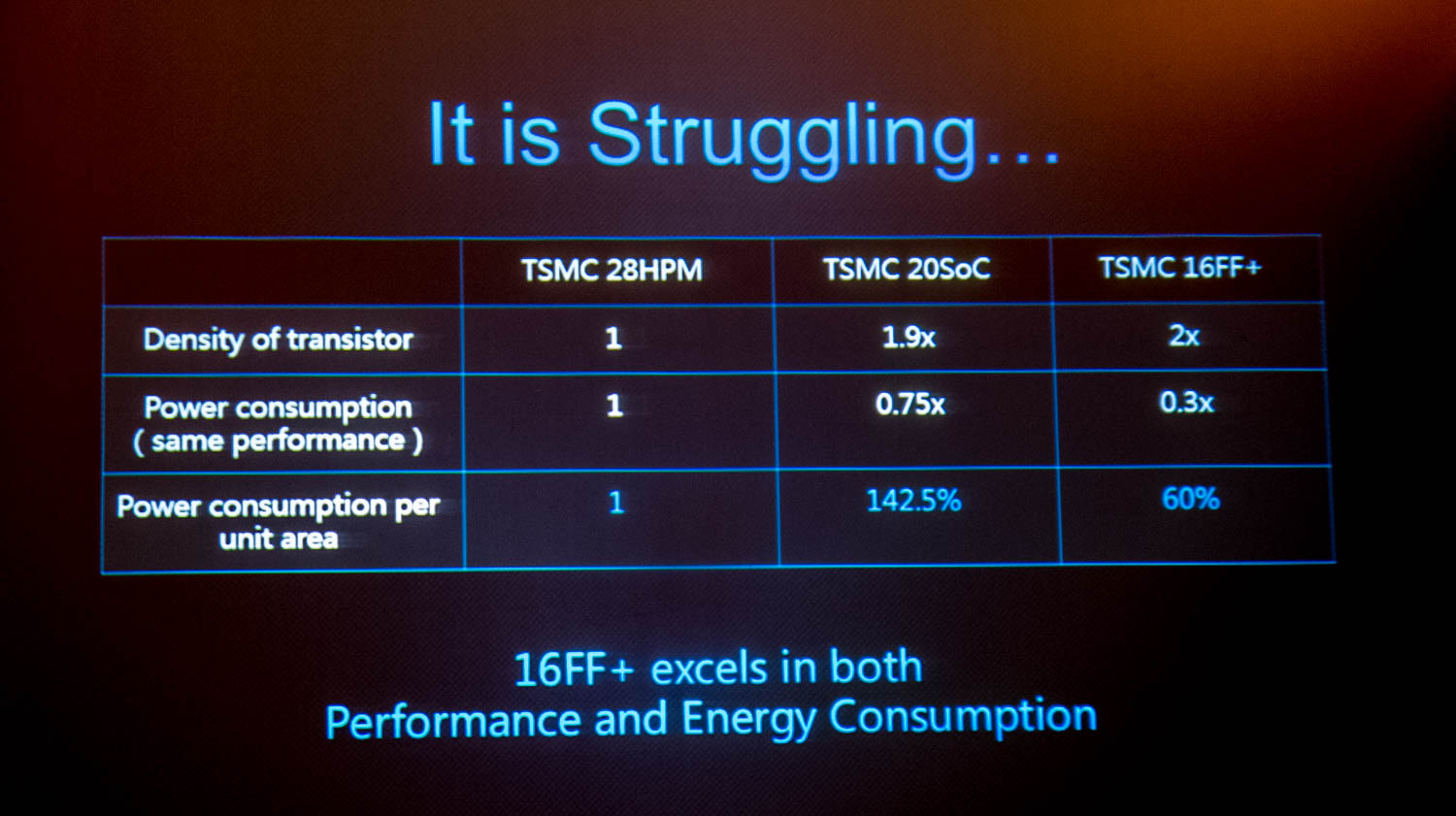
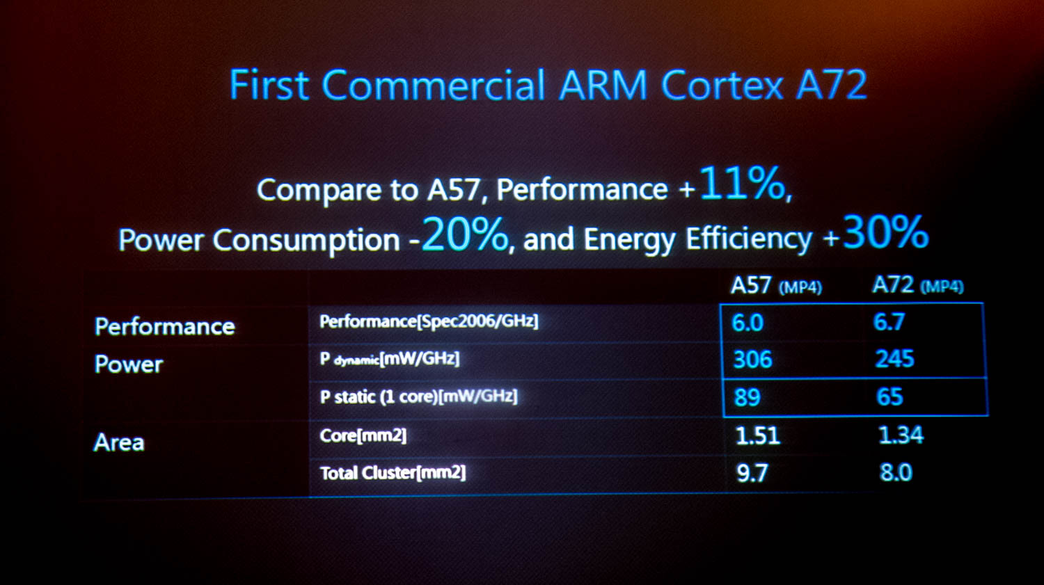
The company was able to show off the implementation area of both an A57 and an A72 on 16FF+. The more interesting number which we can use in an apples-to-apples comparison and put dark silicon into perspective are the A57 figures. Here HiSilicon claims that it an A57 implementation takes up around 9.7mm² - much less than the 13.2 and 15.3mm² we've seen from 20SoC vendors such as Nvidia on the X1 or Qualcomm on the S810 - the point here being that the implementation is much smaller than what the ~8-10% process shrink allows.
Of course, the Kirin 950 uses the more efficient A72 cores which are able to architecturally reduce the block's footprint. As such, the Kirin's big CPU cluster comes in at only 8.0mm², beating the Exynos's 7420 8.88mm² even though Samsung has an advantage on process density.
In terms of power consumption, they also had a slide up demonstrating the power curves of the cores:
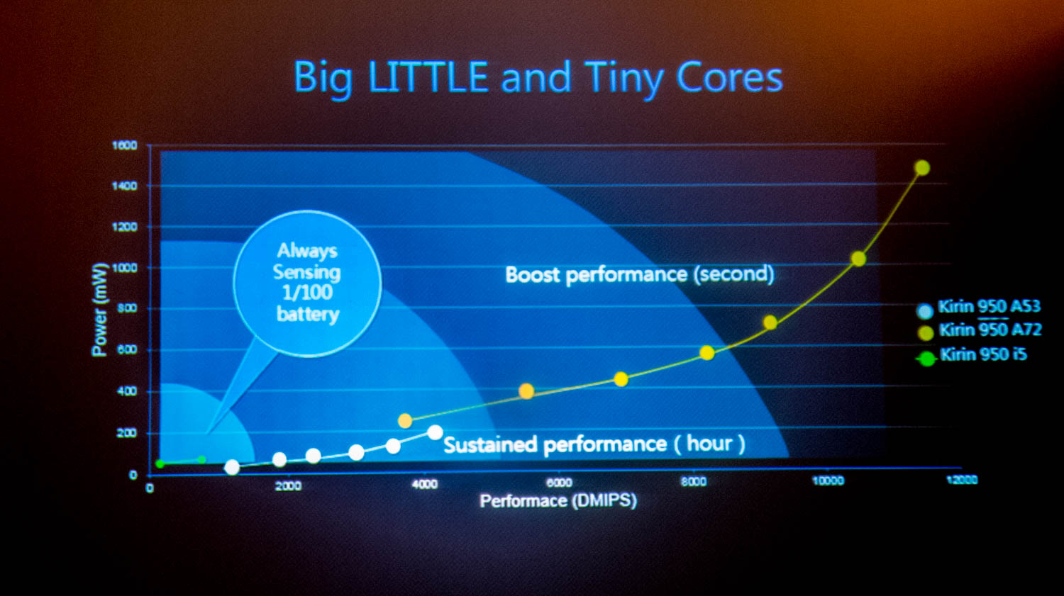
According to the graphic, the A53s max out at around 200mW while the A72s go up to ~1450mW. On the big cores this is somewhat comparable to the Exynos 7420 even though the figures we publish use a different measurement methodology and test-case. HiSilicon uses Dhrystone which I found to use about 10% more power than the power virus which I use for our deep dive power measurement articles.
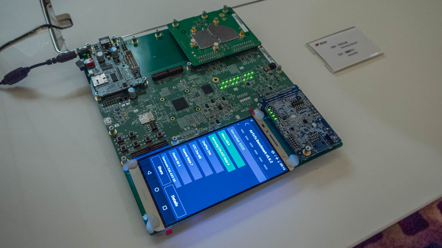
The company had live development demo boards running at the event. While we were unfortunately unable to have more time with them, it does demonstrate the high maturity of the SoC. In fact, we should be seeing products in consumer's hands before the end of the year.
All in all, I think HiSilicon was able to showcase some very significant improvements to the Kirin lineup. I see the Kirin 950 as the true successor to the 920, and it seems that we'll be finally able to move forward in terms of performance and efficiency. While the Kirin still has some rough edges, especially in the aspect of media capabilities, it promises to patch up a lot of the issues that seems to have plagued Huawei's latest flagships. I'm looking forward to getting to test incoming devices with the SoC to see where it places on the competitive landscape.


39 Comments
View All Comments
xype - Thursday, November 5, 2015 - link
It’s 38%, actually, since the percentages compound. 100 * 1.20 = 120, 120 * 1.15 = 138. Still, doesn’t change your point, really. And there is competition, no? It’s just that the fast CPUs are reserved for one line of phones, only. But it’s competition in the sense that it makes others look bad and (hopefully) forces them to improve.Wilco1 - Thursday, November 5, 2015 - link
35% IPC gain in just 3 years (first A15 was in Q3 2012, Galaxy S4 in Q2 2013) is actually a very impressive improvement given they have similar micro architectures (A57 is a 64-bit A15 and A72 is a "tick" of A57). Add the frequency increase and performance has more than doubled in 2-3 years.I don't see how you can possibly claim this is a small gain, especially since x86 performance has completely stagnated in the same period (at best I could get 10-15% gain over the last 3 years if I upgrade my PC).
ssdssd - Thursday, November 5, 2015 - link
Is it?2012 Q3, i7 3770K SPEC CINT2006 base number is 50.3 @ 3.9G turbo
2015 Q3, i7 6770K SPEC CINT2006 base number is 71.3 @ 4.2G turbo
3 year IPC gain is about 30%
Wilco1 - Saturday, November 7, 2015 - link
Most of that "gain" is due to the already completely bogus libquantum result doubling. Note that Sandy Bridge i7 2600 got 49.6 @ 3.8GHz turbo, so that's a better comparison.If you consider the more accurate GCC subtest to avoid these compiler tricks, the gain over 4 years / 5 generations is about 29% overall and just 16.7% in terms of IPC. At about 3.9% a year that's a glacial pace compared to mobile SoCs.
jjj - Thursday, November 5, 2015 - link
When you talk CPU and GPU perf over existing SoCs , maybe there is hope for more given that the existing ones can't sustain max clocks for long.saayeee - Thursday, November 5, 2015 - link
Nice article .. good to see Huawei sharing details about yield, process and power ..Achtung_BG - Thursday, November 5, 2015 - link
Many interesting numbers for area, consumption, yields and power density. I think this is the first LTE modem manufactured with finfets transistors. Well balanced chip from Huawei , 3 cluster configurations with 10 cores is difficult for proper handling and consumes die size.lilmoe - Thursday, November 5, 2015 - link
"For the very vast majority of use-cases and users the GPU isn't a bottleneck and the full potential of more powerful GPUs are never utilized, so the vendors prefer to save die space and thus cost by using less GPU cores"GPU AND other peripherals I might add. It's really sad that only Apple (and Samsung to some extent) packs their SoCs FULL of accelerators, co-processors and other non-off-the-shelf IP. Others just throw a memory controller or a semi-modified generic (yes, GENERIC) ISP/DSP here and there...
I'm not sure, but I believe the problem lies on Android and Android OEMs. It's sad that after all these years of improving hardware acceleration, Android's UI is still *mainly* and heavily CPU bound, which makes it difficult for OEMs to focus on anything other than making Android run "smooth"....... Add to that Google's failure in pushing the ecosystem further beyond "traditional apps".
I seriously gave up on Google. Their business model does NOT benefit from a tightly integrated ecosystem. Only Microsoft can rival Apple there. Hope Microsoft pulls it off.
StrangerGuy - Friday, November 6, 2015 - link
Google wants to flood the market the with low end devices because that's the fastest way to get eyes on screen for advertising bucks.Android devs wants to code for the lowest common denominator hardware for the same exact reason as Google.
Which means there is basically next to no incentive for anybody on the software side of Android to remotely utilize the full potential flagship SoCs, other than bloating the crap out of the UI and uninstallable garbage. Ultimately, that leads the my point that Android has virtually zero value addition outside of recent perfectly usable low end devices to the vast majority of people out there.
leo_sk - Thursday, November 5, 2015 - link
It will be more powerful than snapdragon 820 but less than exynos m1. Only wish to see where helio x30 would stand.