AMD Dives Deep On High Bandwidth Memory - What Will HBM Bring AMD?
by Ryan Smith on May 19, 2015 8:40 AM EST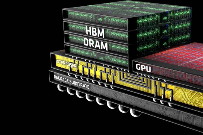
Though it didn’t garner much attention at the time, in 2011 AMD and memory manufacturer Hynix (now SK Hynix) publicly announced plans to work together on the development and deployment of a next generation memory standard: High Bandwidth Memory (HBM). Essentially pitched as the successor to GDDR, HBM would implement some very significant changes in the working of memory in order to further improve memory bandwidth and turn back the dial on memory power consumption.
AMD (and graphics predecessor ATI) for their part have in the last decade been on the cutting edge of adopting new memory technologies in the graphics space, being the first to deploy products based on the last 2 graphics DDR standards, GDDR4, and GDDR5. Consequently, AMD and Hynix’s announcement, though not a big deal at the time, was a logical extension of AMD’s past behavior in continuing to explore new memory technologies for future products. Assuming everything were to go well for the AMD and Hynix coalition – something that was likely, but not necessarily a given – in a few years the two companies would be able to bring the technology to market.
AMD Financial Analyst Day 2015
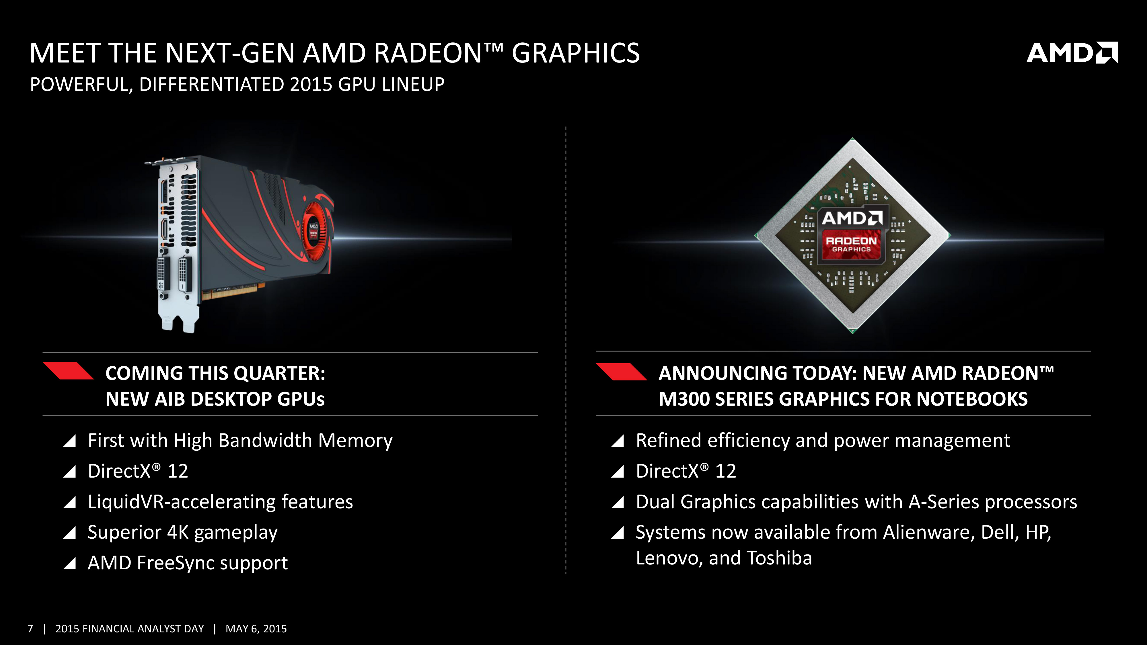
It’s now 4 years later, and successful experimentation has given way to productization. Earlier this month at AMD’s 2015 Financial Analyst day, the company announced that they would be releasing their first HBM-equipped GPU – the world’s first HBM-equipped GPU, in fact – to the retail market this quarter. Since then there have been a number of questions of just what AMD intends to do with HBM and just what it means for their products (is it as big of a deal as it seems?), and while AMD is not yet ready to reveal the details of their forthcoming HBM-equipped GPU, the company is looking to hit the ground running on HBM in order to explain what the technology is and what it can do for their products ahead of the GPU launch later that quarter.
To date there have been a number of presentations released on HBM, including by memory manufactures, the JEDEC groups responsible for shaping HBM, AMD, and even NVIDIA. So although the first HBM products have yet to hit retail shelves, the underpinnings of HBM are well understood, at least inside of engineering circles. In fact it’s the fact that HBM is really only well understood within those technical circles that’s driving AMD’s latest disclosure today. AMD sees HBM as a significant competitive advantage over the next year, and with existing HBM presentations having been geared towards engineers, academia, and investors, AMD is looking to take the next step and reach out to end-users about HBM technology.
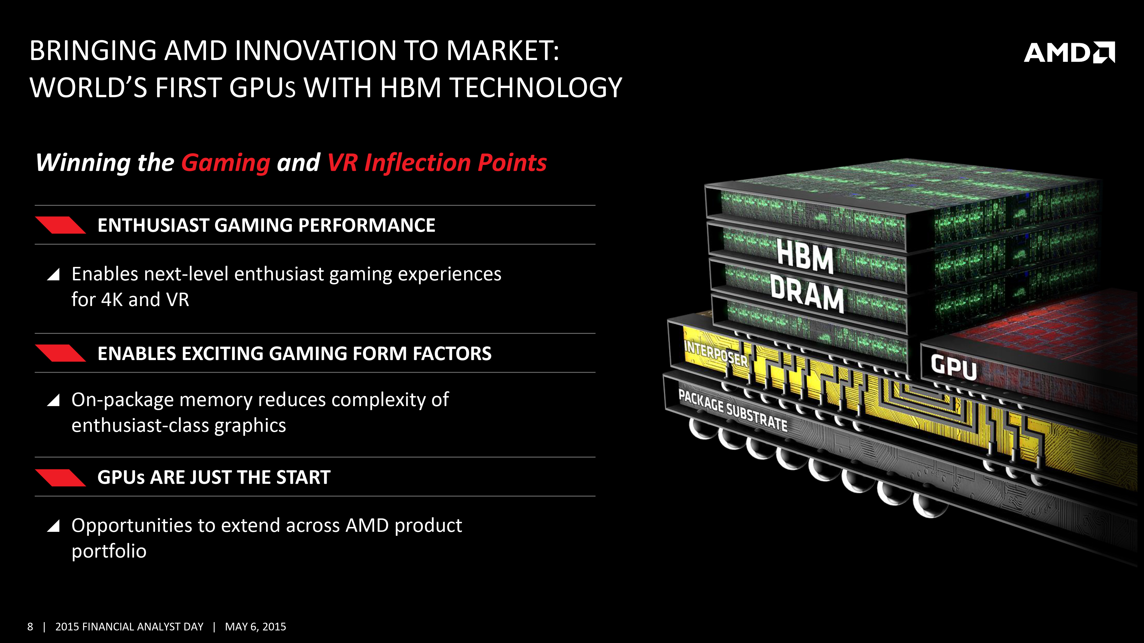
This brings us to the topic of today’s article: AMD’s deep dive disclosure on High Bandwidth Memory. Looking to set the stage ahead of their next GPU launch, AMD is reaching out to technical and gaming press to get the word out about HBM and what it means for AMD’s products. Ideally for AMD, an early disclosure on HBM can help to drum up interest in their forthcoming GPU before it launches later this quarter, but if nothing else it can help answer some burning questions about what to expect ahead of the launch. So with that in mind, let’s dive in.
I'd also like to throw out a quick thank you to AMD Product CTO and Corporate Fellow Joe Macri, who fielded far too many questions about HBM.


163 Comments
View All Comments
ravyne - Tuesday, May 19, 2015 - link
No, not necessarily. AMD isn't exactly allaying any fears by remaining silent so far, but there's a method for chaining two HBM chips together, similar to how chip-select works in normal DDR RAM or SRAMs in embedded systems -- basically you have two chips sharing that 1024-bit memory bus, but there's a separate control signal that indicates which chip the host is talking to. In theory you can chain things along forever with enough chip selects, but a high-performance and highly-parallel bus like HBM is practically limited by signal-propagation latency and misalignment, so using just two chips per HBM bus is more of a practical limitation.looncraz - Tuesday, May 19, 2015 - link
Nope, at least not according to my understanding. In fact, in theory, HBM1 can be configured, at reduced speeds, at well over 8GB. The article even mentions a technical bit of information pertaining to this:"HBM in turn allows from 2 to 8 stacks to be used, with each stack carrying 1GB of DRAM."
From 2GB to 8GB right there, without any trickery. It appears HBM chips need to be used in pairs (otherwise a 2 chip minimum makes no sense), and likely needs to be addressed in pairs (with a 512-bit bus per chip, it would seem). This would indicate there is a two-bit address line which allows from one to four pairs to be individually addressed, or perhaps four binary address lines, whichever they deemed to be more economical and prudent. Either way it appears each stack has a 512-bit data bus.
If correct, you can even use a single 1024-bit bus and interleave on the bus and address 8GB @ 128GB/s maximum. A 2048-bit bus would limit at 16GB @ 256 GB/s, a 3072-bit bus could use 24GB @ 384GB/s, and a 4096-bit bus could use 32GB @ 512GB/s. Interleaving on the bus, though, would increase latency and decrease throughput.
That said, no company, especially not AMD, would design and then bet big on a memory technology that limited them to 4GB without having a solution ready. Everything I mentioned that the HBM chips would be required to support are standard for memory chips made for the last many many decades and was probably included even in the first rough draft for the command protocol without anyone even thinking about it twice. That's just how it works.
It might even be possible to use an 512-bit bus and some latching circuitry to drive HBM. You might even be able to do this with good performance and high capacities without modifying the memory chips at all.
chizow - Wednesday, May 20, 2015 - link
All sounds really good in theory, unfortunately none of the (substantial) source material from AMD/Hynix supports this, nor do the comments from the AMD VP Macri who seems more or less resigned to the fact AMD is going forward with 4GB for HBM1.But in any case, hopefully you won't be too disappointed if it is only 4GB.
looncraz - Wednesday, May 20, 2015 - link
Your comment made me remember that the standard was submitted to JEDEC.JESD235 pertains to HBM (v1), from it I was able to determine that if 8GB was to be supported using 1GB stacks the command interface would have to be duplicated per chip, but the (much larger) data bus could be shared - with some important timing caveats, of course, but that is nothing new for memory controllers (in fact, that is most of what they do), but it is not necessarily something you'd want to do without having already had a working product using the memory technology... and certainly not something you'd bother implementing if you expected higher capacity chips to be available in a year's time...
I finally see how HBM works internally (something that's been lacking from most "technical" articles), and I see why its external interface doesn't follow convention - it's basically an 8/16 bank "up to 8 channel" collection of DRAM chips. Each channel can be addressed separately with a 128-bit data bus and can support 32Gb (4GB) of DRAM.
So HBM uses the relevant addressing lines internally, if at all (vendor specific), and doesn't provide for such a mechanism externally.
From what I'm seeing, it would seem you can build HBM with any width you want, in intervals of 128-bits. Of course, standards are designed to be flexible. That could mean lower powered devices could use 256bit HBM interfaces to save power... unless I'm totally missing something (which is quite likely, it isn't like reading a standards document is the same as reading a quick overview ;-)).
chizow - Thursday, May 21, 2015 - link
Yep exactly, that's where the original 4GB limits for HBM1 came from originally, the JEDEC/Hynix source documents.akamateau - Thursday, May 28, 2015 - link
With Highbandwidth memory depth is not necessary. Of course only the benchmarks will actually show us.And of course DX11 will be useless for this product. HBM was designed to solve a problem! DX12 solves the CPU bottleneck however DX12 benchmarks shows that performance scale sup nicely to 20MILLION + draw calls per second with 6 CPU cores feeding the GPU. When the CPU has 8 coress the performance flatlines and does not get anybetter.
ANAND demonstrated this quite clearly a few weeks back. However HBM will scael far beyond 6 cores as their is more through-put.
Of course that would mean that 390x must be benched using DX12 benchmarks. But that is what they were designed for: Mantle and DX12
akamateau - Thursday, May 28, 2015 - link
You do not need the memory depth with HBM.HBM was designed to solve a problem that becomes apparent with DX12. DX11 does not support multithreaded and multicore gaming. DX12 enables ALL CPU cores to feed the GPU through Asynchronous Shader Pipelines and Asynchronous Compute Engines.
With DX12 GPU performance scales well to 6 cpu cores, beyond that and the GPU drawcall perfomance flatlines: GPU bottleneck. HBM will solve this problem.
DX11 is such a crippling API that anyone even using it to make a decision regarding a $1000 GPU purchase will lkely waste their money.
With DX12 Benching Radeon 390x with HBM will demostrate 400-500% performance increases over DX11.
Do you want to know the facts before you spend your money? Then demand DX12 benchmarks!!
akamateau - Thursday, May 28, 2015 - link
According to AMD's Joe Macri, GDDR5 fed GPUs actually have too much unused memory today. Because to increase GPU memory bandwidth, wider memory interfaces are used. And because wider memory interfaces require a larger amount of GDDR5 memory chips, GPUs ended up with more memory capacity than is actually needed.Macri also stated that AMD invested a lot into improving utilization of the frame buffer. This could include on-die memory compression techniques which are integrated into the GPU hardware itself. Or more clever algorithms on the driver level."http://wccftech.com/amd-addresses-capacity-limitat...
DX11 will not likely allow an HBM AIB to show much of an improvement in performance. Run DX12 games or benchmarks and HBM will rock that AIB!
akamateau - Thursday, May 28, 2015 - link
You do not need the memory depth with HBM.HBM was designed to solve a problem that becomes apparent with DX12. DX11 does not support multithreaded and multicore gaming. DX12 enables ALL CPU cores to feed the GPU through Asynchronous Shader Pipelines and Asynchronous Compute Engines.
With DX12 GPU performance scales well to 6 cpu cores, beyond that and the GPU drawcall perfomance flatlines: GPU bottleneck. HBM will solve this problem.
DX11 is such a crippling API that anyone even using it to make a decision regarding a $1000 GPU purchase will lkely waste their money.
With DX12 Benching Radeon 390x with HBM will demostrate 400-500% performance increases over DX11.
Do you want to know the facts before you spend your money? Then demand DX12 benchmarks!!
A5 - Tuesday, May 19, 2015 - link
Interesting. The article says that AMD is the only anticipated user of HBM1, but are there any rumors on where HBM2 might go?Obvious thing is to make the stacks higher/denser (2-4GB per stack seems more suited to high-end 4K/VR gaming) and increasing the clocks on the interface.