AMD Dives Deep On High Bandwidth Memory - What Will HBM Bring AMD?
by Ryan Smith on May 19, 2015 8:40 AM EST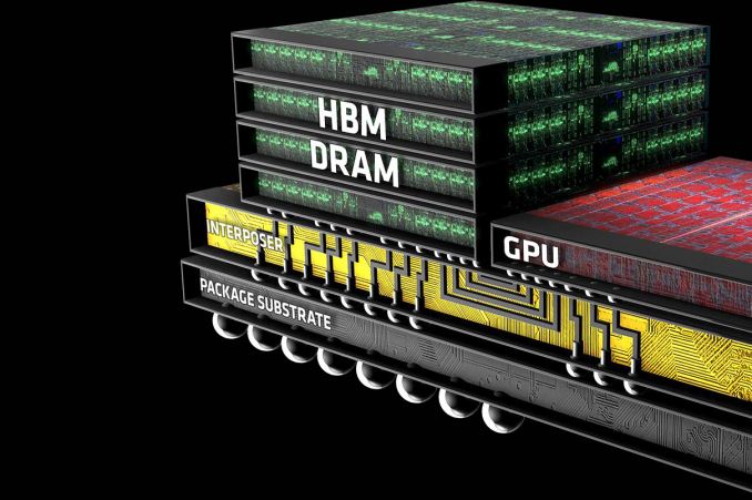
Though it didn’t garner much attention at the time, in 2011 AMD and memory manufacturer Hynix (now SK Hynix) publicly announced plans to work together on the development and deployment of a next generation memory standard: High Bandwidth Memory (HBM). Essentially pitched as the successor to GDDR, HBM would implement some very significant changes in the working of memory in order to further improve memory bandwidth and turn back the dial on memory power consumption.
AMD (and graphics predecessor ATI) for their part have in the last decade been on the cutting edge of adopting new memory technologies in the graphics space, being the first to deploy products based on the last 2 graphics DDR standards, GDDR4, and GDDR5. Consequently, AMD and Hynix’s announcement, though not a big deal at the time, was a logical extension of AMD’s past behavior in continuing to explore new memory technologies for future products. Assuming everything were to go well for the AMD and Hynix coalition – something that was likely, but not necessarily a given – in a few years the two companies would be able to bring the technology to market.
AMD Financial Analyst Day 2015
It’s now 4 years later, and successful experimentation has given way to productization. Earlier this month at AMD’s 2015 Financial Analyst day, the company announced that they would be releasing their first HBM-equipped GPU – the world’s first HBM-equipped GPU, in fact – to the retail market this quarter. Since then there have been a number of questions of just what AMD intends to do with HBM and just what it means for their products (is it as big of a deal as it seems?), and while AMD is not yet ready to reveal the details of their forthcoming HBM-equipped GPU, the company is looking to hit the ground running on HBM in order to explain what the technology is and what it can do for their products ahead of the GPU launch later that quarter.
To date there have been a number of presentations released on HBM, including by memory manufactures, the JEDEC groups responsible for shaping HBM, AMD, and even NVIDIA. So although the first HBM products have yet to hit retail shelves, the underpinnings of HBM are well understood, at least inside of engineering circles. In fact it’s the fact that HBM is really only well understood within those technical circles that’s driving AMD’s latest disclosure today. AMD sees HBM as a significant competitive advantage over the next year, and with existing HBM presentations having been geared towards engineers, academia, and investors, AMD is looking to take the next step and reach out to end-users about HBM technology.
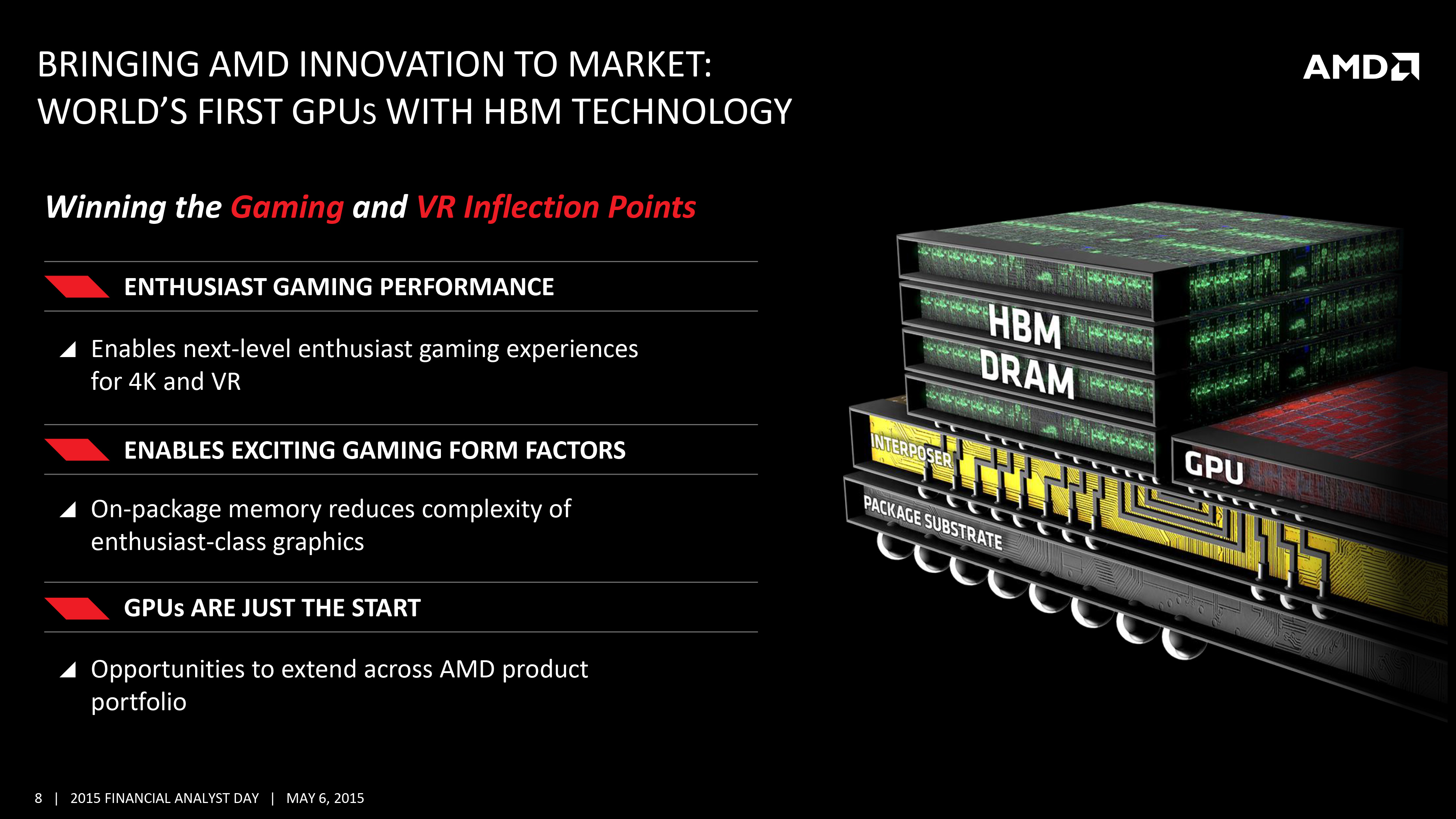
This brings us to the topic of today’s article: AMD’s deep dive disclosure on High Bandwidth Memory. Looking to set the stage ahead of their next GPU launch, AMD is reaching out to technical and gaming press to get the word out about HBM and what it means for AMD’s products. Ideally for AMD, an early disclosure on HBM can help to drum up interest in their forthcoming GPU before it launches later this quarter, but if nothing else it can help answer some burning questions about what to expect ahead of the launch. So with that in mind, let’s dive in.
I'd also like to throw out a quick thank you to AMD Product CTO and Corporate Fellow Joe Macri, who fielded far too many questions about HBM.


163 Comments
View All Comments
WinterCharm - Tuesday, May 19, 2015 - link
Exactly. And science and common sense have shown again and again, if you eliminate the bottlenecks, you can get significant performance gains.That's why SSD's are so great.
AndrewJacksonZA - Thursday, May 28, 2015 - link
What @dew111 said.i7 - Tuesday, May 19, 2015 - link
Wouldn't you see higher memory configs much like the 970 memory config 'fiasco' with greater than 4GB on another substrate or another entirely different configuration?dew111 - Tuesday, May 19, 2015 - link
No. The current HBM stacks come in a fixed capacity, and the Fiji chip will only have so many lanes. Also, it is unlikely an OEM would venture into designing (and funding) their own interposer; this probably won't happen for at least a few years (if ever).akamateau - Monday, June 8, 2015 - link
Actually an OEM can not design an Interposer with a memory controller. AMD owns that patent.Interposer having embedded memory controller circuitry
US 20140089609 A1
" For high-performance computing systems, it is desirable for the processor and memory modules to be located within close proximity for faster communication (high bandwidth). Packaging chips in closer proximity not only improves performance, but can also reduce the energy expended when communicating between the processor and memory. It would be desirable to utilize the large amount of "empty" silicon that is available in an interposer. "
AMD has pretty sewn up the concept of an Interposer being just a substarte with vias to stack and connect silicon.
Besides it would also be unlikely for OEM to be able to purchase unpackaged cpu or memory silicon for their own stacks. And why? Their manfacturing costs would be far higher
eachus - Friday, May 22, 2015 - link
Don't forget the HBM1 vs. HBM2 change/upgrade that is coming. Will HMB2 show up late this year? Or early next year? Your guess. AMD will then be able to ship cards with twice the bandwidth--and four times the memory. My guess is that AMD plans a "mid-life kicker" for Fiji later this year taking it to 8 GBytes but still at HBM1 clock speeds. Then Greenland comes along with 16 Gig and HBM2 speeds.BTW don't knock the color compression technology. It makes (slightly) more work for the GPU, but reduces memory and bandwidth requirements. When working at 4K resolutions and beyond, it becomes very significant.
chizow - Tuesday, May 19, 2015 - link
GTA5 does go over 4GB at 1440p, as do a number of other next-gen games like Assassin's Creed Unity, Shadows of Mordor, Ryse, I am sure Witcher 3 does as well. 6GB is probably safe for this gen until 14/16nm FinFET, 8GB safest, 12GB if you want no doubts. We also don't know what DX12 is going to do to VRAM requirements.Its not about fitting the actual frame buffer, its about holding and storing textures locally in VRAM so that the GPU has access them without going to System RAM or worst, local storage. Hi-Res 4K and 8K textures are becoming more common which increases storage footprint 4 fold and 16 fold over 2K, so more VRAM is always going to be welcome.
silverblue - Tuesday, May 19, 2015 - link
That compression had better be good, then.testbug00 - Tuesday, May 19, 2015 - link
According to NVidia, without gameworks, 1440p at max settings 980 is the recommended card. And with gameworks Titan X/SLI 970.2160p w/out gameworks recommend Titan X/SLI 980. Even at 2160p w/ Gameworks they still recommend 980 SLI.
Based on that my WAG is that TWIII uses under 4GB of VRAM at 2160. I'm guessing bringing Gameworks in pushes it just near the 4GB limit on 980. Probably in the 39xx range.
chizow - Tuesday, May 19, 2015 - link
Can't say for sure as I don't have TW3 yet, but based on screenshots I wouldn't be surprised at all to see it break 4GB. In any case, games and drivers will obviously do what they can to work around any VRAM limitations, but as we have seen, it is not an ideal situation. I had a 980 and 290X long enough to know there were plenty of games dancing close enough to that 4GB ceiling at 1440p to make it too close for comfort.