Intel Releases Broadwell-U: New SKUs, up to 48 EUs and Iris 6100
by Ian Cutress on January 5, 2015 10:00 AM EST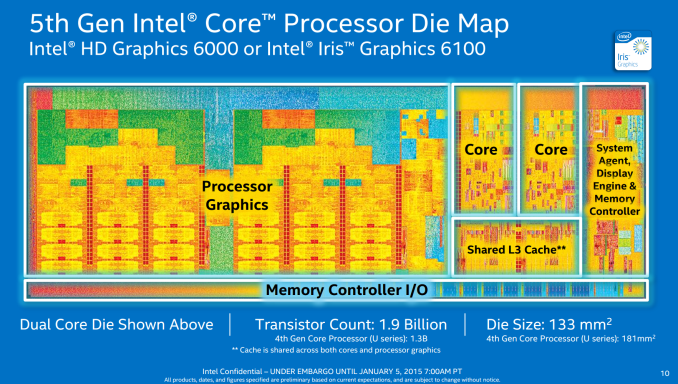
As part of the CES cavalcade of announcements, after launching Core-M back in September, Intel is formally releasing their next element of the 14 nanometer story: Broadwell-U. As the iterative naming over Haswell-U suggests, Broadwell-U will focus on dual-core 15W and 28W units from Celeron to Core i7 using 12 to 48 execution units for the integrated graphics. A Broadwell-U processor should drop into any existing Haswell-U equivalent design (i3 to i3) due to pin and architecture compatibility, albeit with a firmware update.
As with any node change, the reduction to 14nm affords the usual benefits: more transistors per unit area, lower power consumption for a given design, or the potential to increase performance. Ryan covered the details of Intel’s 14nm architecture back as part of the IDF launch, as well as a good deal of the Broadwell architecture itself. The launch today is in essence a specification list with a few extra details, along with potential release dates for Broadwell-U products. The CPUs are already shipping to partners for their designs.
There will be several combinations possible throughout the Broadwell line, but the most important distinctions are:
28W with GT3, Iris 6100 Graphics (48 Execution Units)
15W with GT3, HD 6000 Graphics (48 Execution Units)
15W with GT2, HD 5500 Graphics (23 Execution Units for low i3, 24 for others)
15W with GT1, HD (Broadwell) Graphics (12 Execution Units)
The graphics move up to Generation 8, and a lot of architectural detail into this was given by Intel and IDF San Francisco in September 2014 of which some of the important points are highlighted here.
The New SKUs
Without further delay, the list of the new processors is as follows:
| CPU | Cores | Base Freq (GHz) | 1C (GHz) | 2C (Ghz) | EUs | GPU Base / Max Freq (GHz) |
LPDDR3 / DDR3 Support (MHz) |
L3 Cache | cTDP Down | vPro | 1K $ |
| Intel Broadwell-U 28W + Iris 6100 Graphics |
|||||||||||
| Core i7-5557U | 2 / 4 | 3.1 | 3.4 | 3.4 | 48 | 300/1100 | 1866/1600 | 4MB | 23W | No | $426 |
| Core i5-5287U | 2 / 4 | 2.9 | 3.3 | 3.3 | 48 | 300/1100 | 1866/1600 | 3MB | 23W | No | $315 |
| Core i5-5257U | 2 / 4 | 2.7 | 3.1 | 3.1 | 48 | 300/1050 | 1866/1600 | 3MB | 23W | No | $315 |
| Core i3-5157U | 2 / 4 | 2.5 | 2.5 | 2.5 | 48 | 300/1000 | 1866/1600 | 3MB | 23W | No | $315 |
| Intel Broadwell-U 15W + HD 6000 Graphics |
|||||||||||
| Core i7-5650U | 2 / 4 | 2.2 | 3.2 | 3.1 | 48 | 300/1000 | 1866/1600 | 4MB | 9.5W | Yes | $426 |
| Core i7-5550U | 2 / 4 | 2.0 | 3.0 | 2.9 | 48 | 300/1000 | 1866/1600 | 4MB | 9.5W | No | $426 |
| Core i5-5350U | 2 / 4 | 1.8 | 2.9 | 2.7 | 48 | 300/1000 | 1866/1600 | 3MB | 9.5W | Yes | $315 |
| Core i5-5250U | 2 / 4 | 1.6 | 2.7 | 2.5 | 48 | 300/950 | 1866/1600 | 3MB | 9.5W | No | $315 |
| Intel Broadwell-U 15W + HD 5500 Graphics |
|||||||||||
| Core i7-5600U | 2 / 4 | 2.6 | 3.2 | 3.1 | 24 | 300/950 | 1600/1600 | 4MB | 7.5W | Yes | $393 |
| Core i7-5500U | 2 / 4 | 2.4 | 3.0 | 2.9 | 24 | 300/950 | 1600/1600 | 4MB | 7.5W | No | $393 |
| Core i5-5300U | 2 / 4 | 2.3 | 2.9 | 2.7 | 24 | 300/900 | 1600/1600 | 3MB | 7.5W | Yes | $281 |
| Core i5-5200U | 2 / 4 | 2.2 | 2.7 | 2.5 | 24 | 300/900 | 1600/1600 | 3MB | 7.5W | No | $281 |
| Core i3-5010U | 2 / 4 | 2.1 | 2.1 | 2.1 | 23 | 300/900 | 1600/1600 | 3MB | 10W | No | $281 |
| Core i3-5005U | 2 / 4 | 2.0 | 2.0 | 2.0 | 23 | 300/850 | 1600/1600 | 3MB | 10W | No | $275 |
| Intel Broadwell-U 15W + HD (Broadwell) |
|||||||||||
| Pentium 3805U | 2 / 2 | 1.9 | 1.9 | 1.9 | 12 | 100/800 | 1600/1600 | 2MB | 10W | No | $161 |
| Celeron 3755U | 2 / 2 | 1.7 | 1.7 | 1.7 | 12 | 100/800 | 1600/1600 | 2MB | 10W | No | $107 |
| Celeron 3205U | 2 / 2 | 1.5 | 1.5 | 1.5 | 12 | 100/800 | 1600/1600 | 2MB | 10W | No | $107 |
_thumb.png)
_thumb.png)

There are some clear patterns in the product line. Every unit apart from the Pentium and Celerons has hyperthreading, putting most of the line in a dual core, quad thread scenario. This also ties in with the Pentium and Celeron’s use of HD (Broadwell) graphics, which is a 24 EU design with half of each subslice disabled. The speeds of the Pentium and Celerons are also cut back, despite the 15W TDP and high cTDP down, ensuring that these are the bargain basement units of the line.
vPro will only be enabled on i7-56x0U and i5-53x0U series, giving a range if HD 6000 or HD 5500 is needed, however there is no vPro Iris 6100 part being released. The HD 5500 parts will have a cTDP Down of half their original TDP, allowing 7.5W designs to also take advantage of Broadwell-U.
The Core i3 15W SKUs have an odd combination involving 23 EUs rather than the 24 EUs that the die is designed with, presumably in order to keep yields higher it gives Intel a chance to still sell those with a single defect. This produces a lop-sided EU design within the configuration, which has its own implications, and we are requesting more detail from Intel as to how this is managed in the firmware.
A positive point for 6x00 series graphics SKUs is the memory compatibility on LPDDR3, with these units (having an 5 or an 8 in the 00x0 name) allowing 1866 MHz memory. As our previous Haswell desktop memory testing has shown a small bump away from 1600 MHz DRAM can give a good performance boost when it comes to graphics, especially when the memory speed between CPU and DRAM is the main bottleneck. I would be interested in exploring the difference with this for sure.
It might come across as somewhat surprising that a 15W CPU like the i7-5650U has a 2.2 GHz base frequency but then a 3.2 GHz to 3.1 GHz operating window, and yet the i7-5557U has a 3.1 GHz base with 3.4 GHz operating for almost double the TDP. Apart from the slight increase in CPU and GPU frequency, it is hard to account for such a jump without point at the i7-5650U and saying that ultimately it is the more efficient bin of the CPUs. So while the 28W models will get the glory in terms of performance, there are a number of models that can offer just under that performance but for just over half the power rating. This obviously levels battery life for the more efficient design as a significant jump, depending on how the system as a whole is used.
The Dies and Packaging
Broadwell-U will be derived from two main dies. The larger design contains the full 48 EU (two common slices with 6x8 EU sub-slices all in) configuration for 1.9 billion transistors in 133 mm2, while the 24 EU design (one common slice, 3x8 sub-slices) will measure 1.3 billion transistors in 82 mm2.
This puts the size of one common slice with 3x8 sub-slices at 600 million transistors / 49 mm2, and thus the die without the graphics subsystem at all at 700 million transistors for 33 mm2. This would mean the cores, the Last Level Cache, the IO and memory controller all fit into the 700 million.
Compared to Haswell-U, Intel provided the following data:
Broadwell-U with HD 5500 (24 EU) has 240M more transistors than Haswell-U with HD 4400 (20 EU)
Broadwell-U with HD 6000 (48 EU) has 600M more transistors than Haswell-U with HD 5000 (40 EU)
Unfortunately calculating the increases for separate parts is a little more difficult than just comparing numbers due to the different elements of the new graphics, known as Intel Gen 8.
In terms of the packaging for the dies, we also have some shots of those to share:
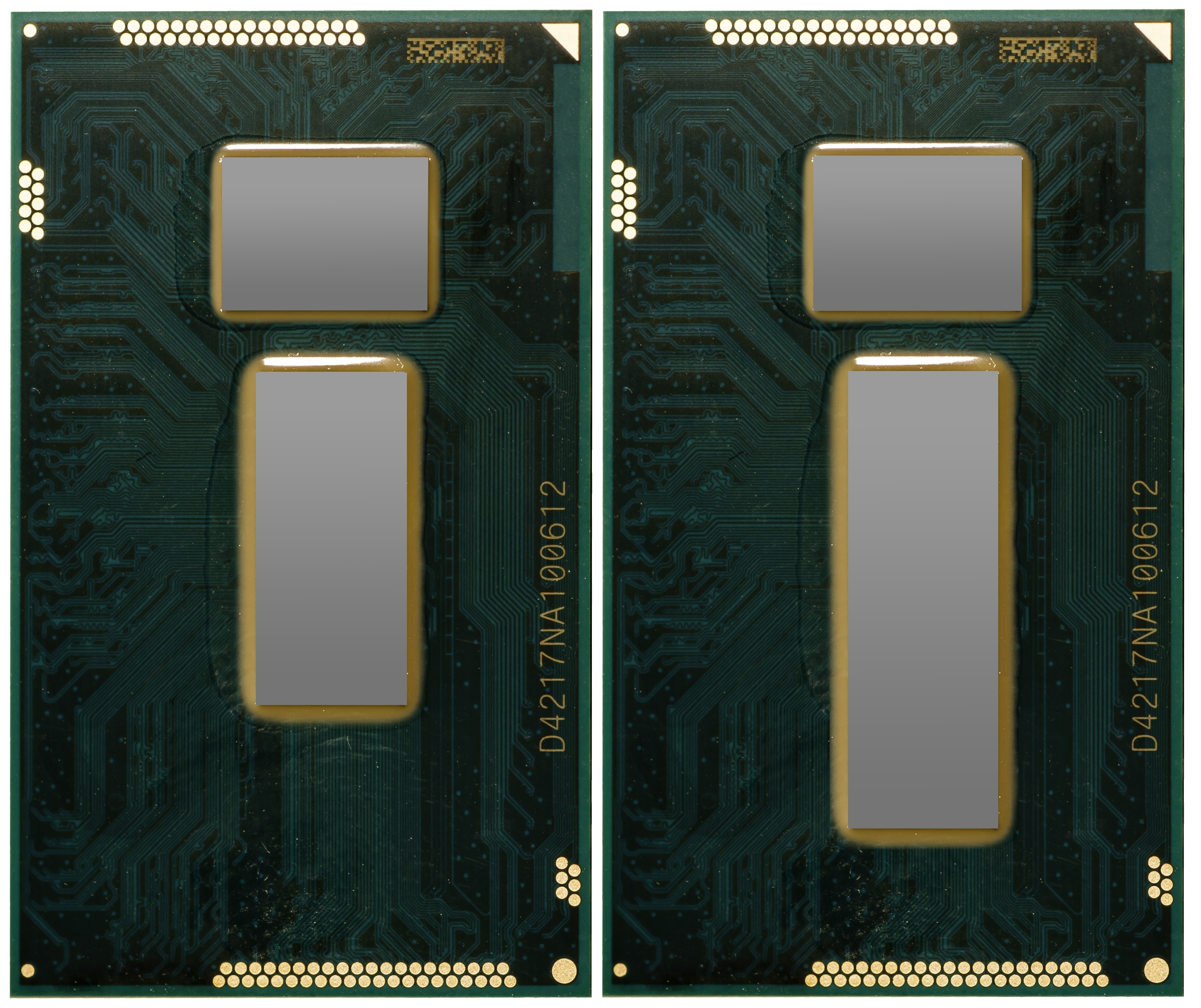
On the left is the 2+2 configuration, giving two cores and GT2 (24 EUs), while on the right is the 2+3 package. The silicon on top is the Platform Controller Hub, discussed later.


85 Comments
View All Comments
Jaybus - Monday, January 5, 2015 - link
Huh? Peak FP32 for x1 is 512 GFlops, substantially less than 48 EU Broadwell-U.name99 - Tuesday, January 6, 2015 - link
BUT Intel offer a coherent single address space for GPU and CPU compute. This is an important step on the path to practical commonplace heterogeneous computing. As far as I know nV aren't offering that in X1.(I'd be curious to know if Imagination are offering it in Rogue 7, because Apple are probably the company that's best set to put all the pieces of this together, from the hardware through the OS to the language+dev tools to the frameworks' but if IMG aren't on track, Apple are kinda screwed. Of course Apple COULD be preparing their mythical self-designed GPU...)
There's plenty to be irritated about with Broadwell, but let's praise the improvements that really are a good foundation for the future, and this is primary among them.
stephenbrooks - Tuesday, January 6, 2015 - link
GFlops not TFlops! And at FP32 the Tegra X1 peaks at 512 Gflops (source: http://anandtech.com/show/8811/nvidia-tegra-x1-pre... ).tipoo - Sunday, January 18, 2015 - link
*Twitch*Argh. The X1 gflop number you just gave is for half precision, it's their double speed FP16 mode. And then you're going and comparing that to a full precision number.
MattCoz - Monday, January 5, 2015 - link
I'm really interested to see what kind of performance improvement can be seen over my current Ivy Bridge i5-3317U. I really want to upgrade my laptop for numerous reasons, but after 2 years I'm looking for more than just a marginal increase in performance. I was very disappointed when Lenovo went with the Core M for the Yoga 3.TiGr1982 - Monday, January 5, 2015 - link
I have this same Core i5-3317U in Surface Pro 1 (1st gen, it works without throttling there, but two CPU fans are audible under heavy load). I believe, CPU-wise, you won't get really big improvements with Broadwell-U over Ivy-U. GPU-wise, however, Broadwell-U will be way faster.So, it depends on what you are interested in more: CPU progress, GPU progress, or both.
III-V - Monday, January 5, 2015 - link
I'm in the same boat. Think I have the same processor, too.I am looking at getting the inevitable Surface Pro 4. It looks like I'll be able to get the same CPU performance (assuming it's Broadwell-Y), and a fair bit better GPU performance, with much improved battery life. Should be good for my needs... Don't need too much number crunching power on the thing, and the graphics are a real sore spot on my Asus S400CA.
nwarawa - Monday, January 5, 2015 - link
I am concerned about the Broadwell Pentiums and Celerons overlapping with the new Cherry Trail.Up until now, Baytrail and Ivybridge Celerons have been sold in similarly priced systems. The Celeron might use a bit more power, but in a cheap laptop, or especially a little ITX box, it was worth it for the extra performance. The 1.5 IvyBridge cores still hold a noticeable lead over a Baytrail core at 2.6 (boost). They shared the same GPU generation, but the Celeron had 6 EUs to the Baytrail's 4 EUs, plus ran at a higher clock.
Now, apparently CherryTrail is going to have 16 EUs to Broadwell Celeron's 12 EUs. They both will have dual-channel LPDDR3-1600 interfaces, so unless the GT1 is clocked significantly higher, this will be the first time an Atom has a better GPU than its mainstream contemporary.
As for the CPU portion, for years the cheapest Celeron U has hardly budged in clockrate, from the 1.4 Sandybridge to the new 1.5 Broadwell. So these chips' upgrades have depended almost entirely on process improvements. The process improvements from BayTrail to CherryTrail sound a bit more aggressive than those from Haswell to Broadwell. So, if Intel ends up clocking the CherryTrail higher too (say, 2.8boost), we may also have situation were the CherryTrail has near CPU performance parity with the Broadwell Celeron.
naloj - Monday, January 5, 2015 - link
Looks like Intel has published the specs of the Broadwell-U NUC line:http://www.intel.com/content/www/us/en/nuc/product...
ayejay_nz - Monday, January 5, 2015 - link
Thanks a lot for this link!