AMD’s Big Bet on ARM Powered Servers: Opteron A1100 Revealed
by Stephen Barrett on August 11, 2014 12:00 PM EST- Posted in
- SoCs
- IT Computing
- AMD
- Arm
- Opteron
- server
- Enterprise CPUs
- Opteron A1100
It has been a full seven months since AMD released detailed information about its Opteron A1100 server CPU, and twenty two months since announcement. Today, at the Hot Chips conference in Cupertino, CA, AMD revealed the final pieces about its ARM powered server strategy headlining the A1100.
The Case for Low Power Server CPUs
Before we discuss the new Opteron A1100 details, let us review the background of why AMD designed an ARM powered CPU. It all comes down to the devices and services we now take for granted: cell phones, tablets, cloud storage, and cloud services. AMD presented a slide about a year ago that summed it up nicely.
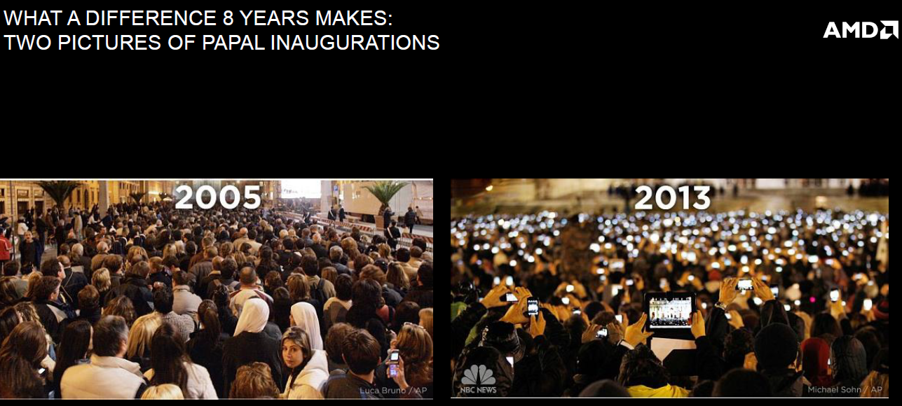
The amount of internet users is growing by 8 to 12% every year. Apple, Google, Microsoft, Facebook, you-name-it, all invest huge sums of money into server farms to provide the services we have come to rely on. This trend gains more and more momentum as software companies like Microsoft try to emulate the success of Apple and Google by selling hardware (Apple) and providing free services (Google) that are ad-supported.
Building the infrastructure to support all these devices and users is a massive undertaking. Typically, companies buy traditional high powered servers (read: Intel Xeon) and partition their computing power up between many tasks as needed. However, this isn’t always the best strategy. For IO tasks, you are always bottlenecked by something other than the CPU, so there is not a reason to throw high cost high power CPUs at the problem. For webserver tasks, response time is paramount. However, with the huge number of users connecting, webservers have become an ‘embarrassingly parallel’ problem you can address with multi core CPUs - as long as there is enough muscle behind each CPU.
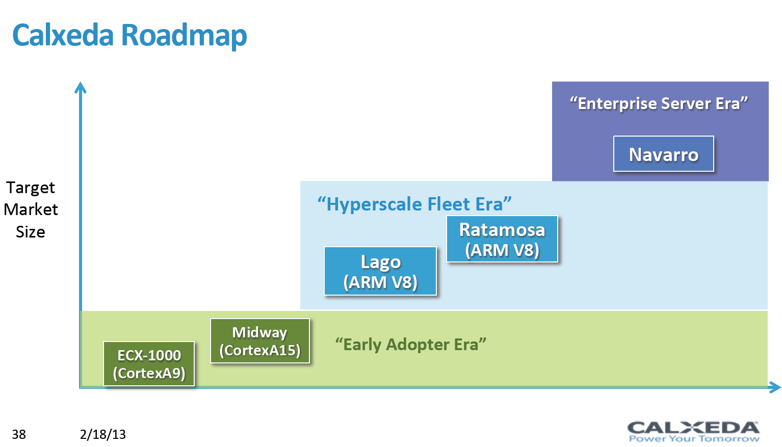
The ‘enough muscle’ issue has hindered previous low power high density webserver attempts. When we tested the Calxeda ARM compute cluster, there were only certain edge cases where it was more efficient than a dual core Xeon server running virtual machines. Calxeda themselves admitted that their processors, utilizing ARM Cortex A9s, were in the early adopter phase of ARM powered webservers. Calxeda stated it wouldn’t be until ARMv8 (where virtualization is supported) and Cortex A57 that ARM based servers would ‘cross the chasm’ and enter the mainstream.
With the Opteron A1100, AMD skipped the early adopter phase and chose something with a higher chance of initial success.
Meet the A1100: CPUs and IO
There are three types of ARM licenses: POP, processor, and architecture. A POP license stands for Processor Optimization Pack and provides the licensee with everything they need to send a chip to the fab. A processor license provides the details of an ARM core like Cortex A9 so you can implement it into your own SoC, but you are not allowed to customize it. Finally, there is the ultimate license, an architecture license. An architecture license provides all details of ARM instruction set (ISA) and CPU implementation so a licensee can implement their own custom CPU core using the ARM ISA however they see fit. AMD is a processor and architecture licensee. If AMD decides it can be competitive by shipping an SoC with an ARM designed CPU (processor license), they can do so without the effort designing their own ARM ISA CPU. If AMD wants to differentiate itself with a custom designed CPU using the ARM ISA, AMD can use its architecture license to do that, similar to Qualcomm’s Krait CPU cores. AMD has decided to do both. Today we discuss its processor license.
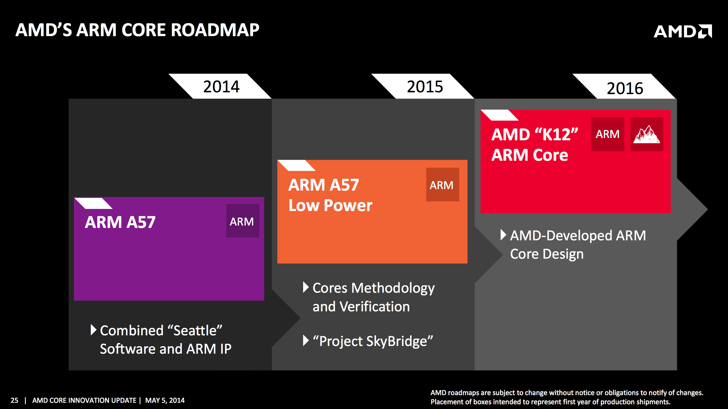
AMD’s first SoC containing an ARM CPU is code named Seattle, the Opteron A1100. Seattle features no less than eight 64-bit ARMv8 ISA, Cortex A57 cores. Depending on availability, this could be the first Cortex A57 CPU to hit any market, not just the server market. AMD will follow up in 2015 with a lower power version that is pin compatible with another x86 CPU, both of which are part of Project Skybridge. In 2016 AMD will leverage its architecture license and ship K12, a fully custom CPU design using the ARMv8 ISA.


Each pair of Cortex A57s in the A1100 shares a 1MB L2 cache (totaling to 4MB of L2), and they all roll up to a shared 8MB L3 cache. To address the server market, all caches are ECC protected except for the L1 instruction cache, which is parity protected instead. Instruction cache protection is not quite as important (invalid instruction just means a pipeline stall). AMD utilizes ARM bus interfaces and debugging support throughout the design. The Cortex A57 also implements cryptography extensions that are quoted by ARM to accelerate things like https by 3-10x over previous ARM designs.
The SoC has a dual channel (2x64-bit) DDR3/4 interface to up to 128GB of 1866MHz memory. Just like the caches, the memory path also supports ECC of the single-bit error correct / double-bit error detect variety. Registered (RDIMM), unregistered (UDIMM), and small-outline (SODIMM) memory modules are support by the A1100 SoC, but actual motherboards will likely support only one type of memory. The same goes for DDR3 vs. DDR4.
As the A1100 is a SoC, it integrates IO directly into the single chip instead of relying on an off-chip IO hub. Integrated components include 8 SATA 3 (6Gb/s) ports, two 10 Gbit Ethernet (10GBASE-KR) ports, one 10/100/1000 Ethernet port, 8 lanes of Gen3 PCI-Express (supporting 8x, 4x/4x, and 4x/2x/2x), I2C, SPI, and UART. The inclusion of this breadth of storage IO (8 SATA3 ports) along with the 2x10 Gbit Ethernet is particularly interesting as it gives us hints of how AMD will position the Opteron A1100 on the market. More on this later.


28 Comments
View All Comments
coburn_c - Tuesday, August 12, 2014 - link
Why are there no 28nm FX products. Why are there no micro atx/mini itx AM3+ boards. Why is AMD walking away from the performance market. Why would anyone buy ARM from AMD when their track record is to walk away from their customers?silverblue - Tuesday, August 12, 2014 - link
There's a lot of "why"s in your post. I doubt they have the money to create a new FX line right now (28nm SHP doesn't clock as highly as 32nm SOI anyway). Their performance CPU lines are not popular enough (and probably too power hungry) to warrant uATX/mITX.As for the last question, AMD have the market experience and are ahead of everybody else in bringing such a product to market. I doubt they'll have their own cake and eat it, but how they get on here will be a good indication for other ARM licensees as to what they can expect from releasing their own products. Besides, if you can't directly compete in traditional markets, you need to possess the agility to look for a market that you can compete in. That is kind of the point - in my eyes - to AMD hiring Rory Read in the first place, and should be answered over the next year.
atlantico - Tuesday, August 12, 2014 - link
AMD probably wants to make sure that the next FX they offer will be an unquestionably worthwhile upgrade. The FX line has been very good, in fact the FX8350 is still the best value chip available for purchase (though the FX8300 is a pretty good value too) - but the competition can offer better performance.Like when the Radeon HD7900 line was introduced, an extremely good value GPU, it still didn't perform as well as the competition and many were reluctant to give credit to that line - but the 7900 GCN chip was a beginning, like the FX8300 line is.
The next major iteration of the architecture must be a worthwhile step up, and I'm sure AMD can deliver on the CPU front as they did on the GPU front, but as the GCN refresh took time, the FX refresh will too.
It will ship when it is ready. AMD is here to stay.
beginner99 - Tuesday, August 12, 2014 - link
Still don't see the point of this. it's niche. Visualization on a full server cores is just as efficient and offers other advantages. Yes it might be cheaper but if the difference of CPU cost usually is negligible in servers running software that costs millions per year.easp - Tuesday, August 12, 2014 - link
If you don't see the point, then you are so far from the target market, you should just skip articles like this in the future.The primary market for this is for orgs that buy servers by the aisle (or data center), particularly those that own most of the software stack that runs on them.
Such people care a lot about power consumption. Balanced system architectures with a good balance between compute, memory bandwidth and I/O tend to be more efficient and can have capital cost advantages as well.
Ammohunt - Thursday, August 14, 2014 - link
Not for OS agnostic highly threaded workloads. I have a lot of backend tasks here where i work that could be offloaded to say a KVM based virtual environment running on ARM. Environmentals are expensive and large blade chassis put a lot of load them.eyours12 - Sunday, August 17, 2014 - link
Cool!cait@asomi.com - Thursday, August 28, 2014 - link
Is the cryptographic co-processor an OpenCL device, or is limited to specific cryptographic functionality. The latter would be a mistake. It takes an ARM design and makes it more like Intel CPUs rather than the approach AMD has been promoting.