NVIDIA Reveals First Details about Project Denver CPU Core
by Anand Lal Shimpi on January 6, 2014 12:08 AM EST- Posted in
- SoCs
- CPUs
- Project Denver
- NVIDIA
- Tegra K1
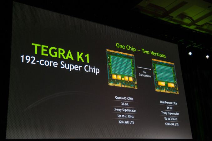
During its CES press conference, NVIDIA revealed its new Tegra K1 SoC will be available in two versions. One version will ship with four ARM Cortex A15s, while the other will ship with two NVIDIA designed Denver CPU cores. We don't know much about Denver other than it's a custom 7-wide superscalar 64-bit ARMv8 design.
NVIDIA claims very high single and multithreaded CPU performance. It's important to note that the Denver version only comes with two cores, something we've argued is likely the more optimal use of die area in mobile. Max frequencies top out at 2.5GHz. Given that NVIDIA has silicon back already I suspect this is a 28nm design. The L1 cache is 128KB + 64KB (I$ and D$?).
The Denver CPU cores will be paired with a 192 CUDA core Kepler implementation (1 SMX). No word on differences in power or performance. The Cortex A15 version of Tegra K1 will be available in 1H 2014, while the Denver version will be available in 2H. The two SoCs are pin-compatible, indicating that there won't be any difference in memory interface width.


36 Comments
View All Comments
twizzlebizzle22 - Monday, January 6, 2014 - link
Do we think Nvidia are going to meet the power and clock requirements in these implementations when it comes to the OEMs and mass produced chips with differing bins?Also can anyone explain or link me to some information on what a 3 or 7 way superscalar is?
dylan522p - Monday, January 6, 2014 - link
How wide an architecture is.winterspan - Monday, January 6, 2014 - link
I'm no expert, but I believe it refers to how many instructions can be issued (i.e. worked on) simultaneouslyKrysto - Monday, January 6, 2014 - link
Someone posted this on Beyond3d:5 watts related to perf numbers in the table(365 Gflops), GPU should work at ~1Ghz to achieve those flops, it's definitely not for smartphones or even tablets, but rather for cars and chromebooks, but considering last summer demo with 1 watt GPU power consumption it should be scalable down to phones, that's why you can observe POP package here - http://www.nvidia.com/object/tegra-k1-processor.ht...
Wow. It needs to reach 1 Ghz to get that performance? If that's true, then FU, Nvidia! I HATE it when both Intel and Nvidia do this. They mislead people with their benchmarks and "theoretical max performance" numbers or some crap like that, when in reality you're not going to be able to utilize that much performance because your devices will get TOO HOT within MINUTES!.
I have an Nvidia GPU in my laptop, and it's useless. It advertises 3x the performance of the Sandy Bridge GPU, but when I play games, after about 30 minutes, it throttles to about half of that performance or less, making it barely any better than the Intel GPU. Then what the hell is the point of all that performance, if I can't USE it?
I thought Nvidia learned a lesson with Tegra 4 so they don't make a "tablet chip" that inevitably becomes too performance focused, and draws too much power. It seems they are repeating the mistake with Tegra K1, though, and it won't actually be a "smartphone chip" that can actually be used for more than a few minutes under intense load.
Nvidia has one more shot with Tegra K2 at 16nm FinFET. If they fail to make a proper "smartphone chip" that's efficient even at maximum load, then I'm giving up all hope on Nvidia.
Damn it and I wanted them to do well, because I really think Qualcomm is about to turn bad and become uncompetitive due to its almost market monopoly at the high-end.
twizzlebizzle22 - Tuesday, January 7, 2014 - link
Yeah these benchmarks are all impressive etc but when you see the likes of what qualcom are doing on the "last gen" implementations. As battery tech is only seeing marginal gains its interesting to see the power improvements which can be made throughout the soc. Tech like envelope tracking etc. Personally I don't game on mobile only in the desktop space so I'm interested to see applications and derivatives of the a57 which draw minimal power, I hope the next nexus focuses on a more power efficient chip in favour of chasing the court and clock count. As in the hangout with Peter Greenhalgh he mentioned not pushing the chips above 1.8 - 2.0ghz. I'm sure the 10% performance increase isn't going to be worth it with the extra voltage that needs to be pumped in, its not linear.I'm sticking with my Nexus 5 until a decent power efficient chip is made available whether that's with 16nm FinFET or even on the 20nm space, any mid to high range chip is powerful enough to run android pretty much jank free.
phoenix_rizzen - Thursday, January 16, 2014 - link
Any SoC released since summer 2012 (so Qualcomm Snapdragon S4 Pro or newer) is capable of running vanilla Google Android or AOSP-based Android ROMs "jank free". And, each version of Android since 4.2 has required less resources to provide the same fluidity. Just look at what Motorola was able to do with the Moto X, running dual-core Krait 300 CPUs and older Adreno 320 GPU (aka Snapdragon S4 Pro), for example.However, it takes a very recent SoC (like Snapdragon S600 or newer) to run OEM-skinned Android even slightly janky, with TouchWiz and LG's versions some of the worst offenders. LG's version of Android 4.1.2 runs like molasses compared to Rootbox 4.2.2 or Carbon 4.3.1 on my Optimus G (quad-core Snapdragon S4 Pro).
We don't need faster/more efficient hardware. We need faster/more efficient software that can use all the features of the hardware we already have. The Moto X is an excellent example of this. Motorola's optimised bionic and dalvik libs make the older hardware feel more powerful than it actually is. And many custom ROM devs have ported those to other Qualcomm-based phones with great results. Same with the Adreno drivers; there are heavily-optimised drivers floating around that make even Adreno 320 speed up by 10-20%; again ported to various custom ROMs.