Intel Z77 Panther Point Chipset and Motherboard Preview – ASRock, ASUS, Gigabyte, MSI, ECS and Biostar
by Ian Cutress on April 8, 2012 12:00 AM EST- Posted in
- Motherboards
- Intel
- Biostar
- MSI
- Gigabyte
- ASRock
- Asus
- Ivy Bridge
- ECS
- Z77
Well, today is a day that everyone was expecting but not the most exciting day of the month. Today, Intel officially releases the spate of 7-series chipsets for their 3rd generation Core microarchitecture processors (read—Ivy Bridge), despite the actual release of the processors being another three weeks away. This means that today we can actually look at, test, or purchase the range of motherboards that natively support Ivy Bridge. However, we can’t officially publish all the benchmarks for these products using Ivy Bridge until that date three weeks away (to be honest, we are still testing!). So today we are going to have a good in depth look into the Z77 chipset itself, and the review products we have received to let you know what we think looks good. All these boards today will be fully reviewed, warts and all, with Ivy Bridge, as close to official release as possible.
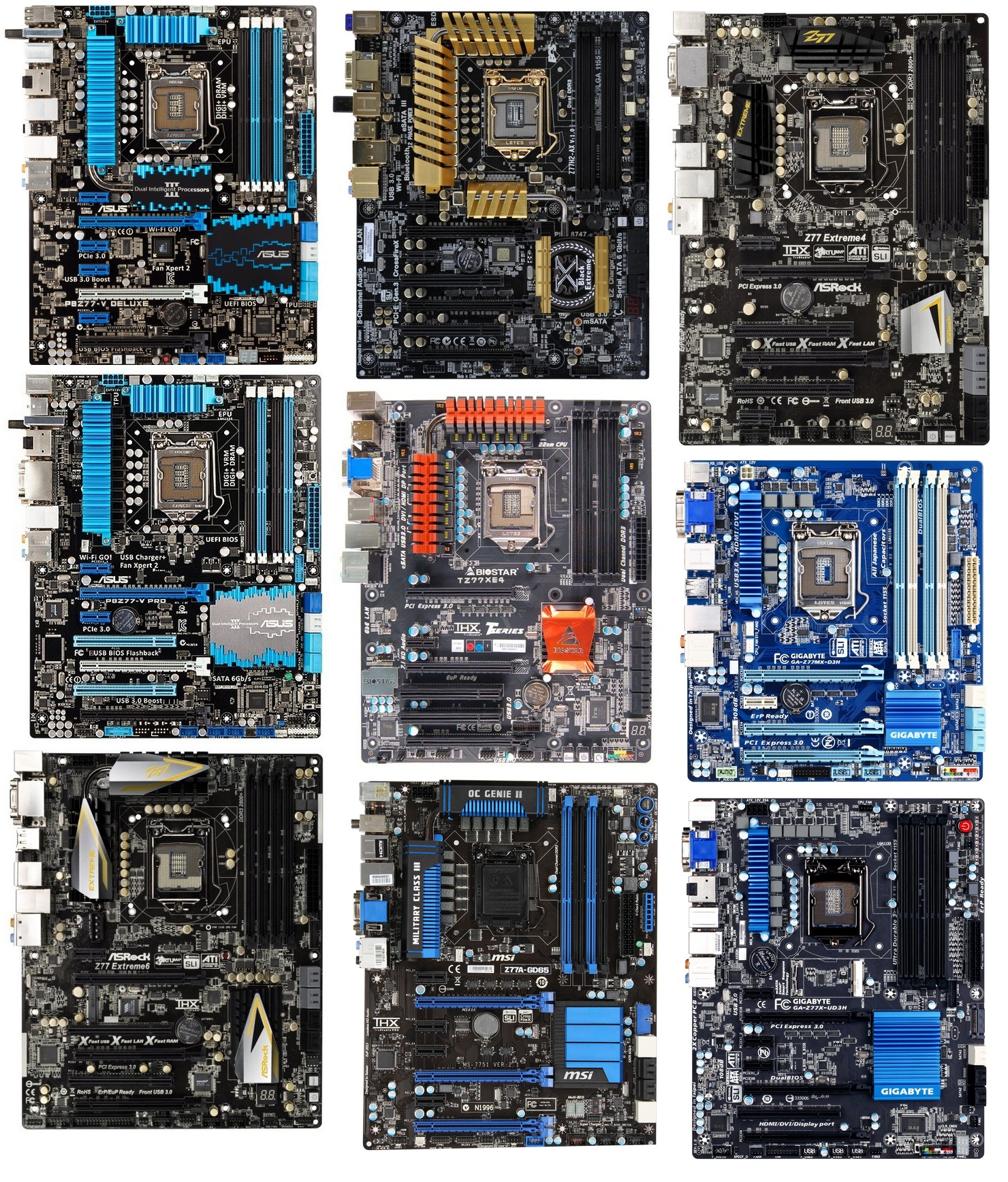
The boards today are from ASRock, ASUS, Gigabyte, MSI, ECS and Biostar. All these boards will natively support Sandy Bridge processors, and be fully upgradeable to Ivy Bridge silicon when the processors are released.
The Z77 Chipset
The important things to note about the Z77 chipset will be its differences to all things Sandy Bridge/Cougar Point, typically in relation to the Z68 platform. Rather than have a split between a chipset with video outputs and a chip without video outputs, all motherboards in the Z77 (and H77) will natively support video outputs (if the motherboard manufacturer wishes to use them). There will also not be a chipset issue as there was back this time last year with Cougar Point—so none of this B2/B3 nonsense that confused consumers.
In comparison to the previous chipsets, what we can see is simple from a table:
| Chipset Comparison | ||||||||
| Z77 | Z75 | H77 | Z68 | P67 | H67 | |||
| CPU Support |
IVB LGA-1155 |
IVB LGA-1155 |
IVB LGA-1155 |
SNB/IVB LGA-1155 |
SNB/IVB LGA-1155 |
SNB/IVB LGA-1155 |
||
| CPU Overclocking | Yes | Yes | No | Yes | Yes | No | ||
| CPU PCIe Config |
1 x16 or 2 x8 or 1 x8 + 2 x4 PCIe 3.0 |
1 x16 or 2 x8 PCIe 3.0 |
1 x16 PCIe 3.0 |
1 x16 or 2 x8 or 1 x8 + 2 x4 PCIe 3.0 |
1 x16 or 2 x8 PCIe 3.0 |
1 x16 PCIe 3.0 | ||
| Processor Graphics Support | Yes | Yes | Yes | Yes | No | Yes | ||
| Intel SRT (SSD caching) | Yes | No | Yes | Yes | No | No | ||
| RAID Support | Yes | Yes | Yes | Yes | Yes | Yes | ||
| USB 2.0 Ports (3.0) | 14 (4) | 14 (4) | 14 (4) | 14 | 14 | 14 | ||
| SATA Total (Max Number of 6Gbps Ports) | 6 (2) | 6 (2) | 6 (2) | 6 (2) | 6 (2) | 6 (2) | ||
| PCIe Lanes | 8 (5GT/s) | 8 (5GT/s) | 8 (5GT/s) | 8 (5GT/s) | 8 (5GT/s) | 8 (5GT/s) | ||
Segregation is quite apparent for the consumer—a Z means you can overclock an appropriate CPU, and a ‘77’ means that you can take advantage of Intel’s SSD smart caching.
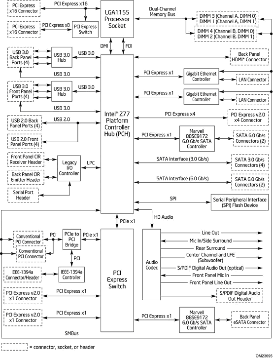
The chipset diagram above shows the layout of the Intel DZ77GA-70K motherboard, showing sixteen PCIe lanes from the processor. The astute will note that only one PCIe lane is coming from the PCH to the PCI Express Switch, which powers the PCIe to PCI bridge (and thus PCI and IEEE1394a) and the PCIe 2.0 x1 ports. This would mean that users of the DZ77GA-70K may experience bandwidth limitations when PCI and PCIe x1 devices are used.
PCIe 3.0
We still have 16 PCIe lanes from the CPU, but with the new chipset these are fully and officially rated at PCIe 3.0 speeds if you have the GPUs to take advantage of this feature. This becomes more apparent in multi-GPU setups, where the 16 lanes are split between the slots. Typically, this will be in the form of x16 for single card, x8/x8 for dual GPU, and x8/x4/x4 at tri-GPU. Having an x4 PCIe 3.0 is equivalent to an x8 PCIe 2.0, but only if you have a card that can take advantage of PCIe 3.0.
Due to this feature with the CPUs, the chipsets will have to adhere to PCIe 3.0 compliance, to deal with the transfers and lane layout design. A novel addition that we will see on many of the high-end boards is a series of onboard chips to increase the number of available lanes. These are known as PCIe 3.0 PLX PXE chips, which increase the number of lanes on the motherboard from 16 to 32—all rated PCIe 3.0. This also raises the cost of the motherboard, perhaps as much as $10-$15, so it is worth thinking long and hard if you really need that tri-GPU setup.
Native USB 3.0
The other long awaited addition found on Panther Point is the native implementation of USB 3.0 that comes directly from the chipset. The chipset will only provide two USB 3.0 headers, giving four ports total, either in the form of rear panel additions or an onboard header (this is at the discretion of the motherboard manufacturer). For many low-end boards, this eliminates the cost of a controller from the product. For high end SKUs that typically have 4-6+ USB 3.0 ports, while it does reduce the number of controllers by two, some PCB real estate will still be utilized by USB 3.0 controllers.
Memory Improvements
The Panther Point chipset comes with a few additional features that may be of benefit to some users. Partially derived from the processors themselves, the chipset now supports DDR3L thanks to its power gated DDR3 interface. This is a primary benefit for the lower end processor and chipset products (that is, all things mobile), but we will see if this moves its way into the mainstream or HTPC versions of Panther Point.
For the high-end power user, the chipset is now geared to handle memory that is more powerful. Again, thanks to the improvement on the new processors, these combined systems should be able to handle (with ease) DDR3-2800 memory. The memory dividers work similar to the gear ratios in Sandy Bridge-E, with users able to call a larger array of memory dividers than before with up to 200 MHz increments. This is of great benefit to the integrated graphics on the new generation processors, which should benefit from the purchase of a higher end memory kit to provide enough bandwidth.
We are still going to play with dual channel memory for the time being on consumer platforms. As this processor change is only a tick (process node decrease), we will have to wait for a tock or two in order for the memory subsystem to change to a larger number of channels. As seen on X58, tri-channel memory/6 slots was fairly cumbersome on motherboards, however on Sandy Bridge-E the quad channel memory (should Intel want to move in this direction) would still allow four slots on the board for an increase in memory bandwidth. However for now, dual channel it is.
If you happen to purchase ASUS for Ivy Bridge, there is also a little treat in store, as they have reworked the memory sub-system. Their new method stunned Intel engineers, but should provide distinct memory speed advantages. Simply put, instead of memory banks being read consecutively, the memory is read in parallel. We are awaiting more detail regarding how this feature works.
Power Consumption and Power Delivery
It has been well documented over the past few months that the top end model of the new processors should have a TDP of 77W. This is just shy of 50 watts less than the top models seen in Sandy Bridge-E, but more importantly, down from 95 watts as shown by the 2600K/2700K processors of Sandy Bridge. This does force a small change with the power delivery on Panther Point/Z77 products.
With less TDP to cater for, the motherboard manufacturers can spend less on the power delivery to get it to work. So there is a chance that the days of '24 phase power’ are long gone, and we will be dealing with less phases. Fewer motherboards will have dual 8-pin 12V connectors, and unless you go high end, may only require one 4-pin 12V connector to get the job done. Obviously if you apply an overclock, having access to more current (and thus more power) is of major benefit, but for the majority of system builders who will run systems at stock, this could represent savings in the construction being passed on to the consumer.
However, this does lend itself to potential issues when used in conjunction with Sandy Bridge processors—having a power delivery system less robust than Z68 could perhaps hinder Sandy Bridge overclocks.
Backwards Compatibility with Sandy Bridge Processors
To confirm what has been said in news articles around the world, the Intel 7-series chipsets will be backwards compatible with the Sandy Bridge (Intel 2nd Generation Core Microarchitecture) processors from the point of sale. All motherboard vendors should have this functionality built into their BIOSes. The beauty lies not in backwards compatibility but in releasing chipsets to take advantage of the new features—this is something AMD has done well with in the past.
In addition, a significant number of Intel 6-series chipsets (P67, Z68) should be forwards compatible with the Ivy Bridge processors, pending a BIOS update. Thus, current Sandy Bridge processor owners wishing to upgrade should make sure they have an appropriate BIOS before installing a new processor in their 6-series motherboard.


145 Comments
View All Comments
extide - Tuesday, April 10, 2012 - link
Do you even know what it means to preempt a frame? Cavalcade is describing the technology correctly. He is explaining pretty much the same thing as you are but you just don't get it..Also separate input and rendering modules means a lot. Typically a game engine will have a big loop that will check input, draw the frame, and restart (amongst other things of course) but to split that into two independent loops is what he is talking about.
Iketh - Wednesday, April 11, 2012 - link
You really should look up "preemption." This is not what is happening... CLOSE, but not quite. Preemption is not the right word at all. This makes him incorrect and I kindly tried explaining. You are incorrect in backing him up and then accusing me of being inept. Guess what that makes you?On top of that, he's also not talking about splitting input and rendering into two loops. Not even close. How did you come up with this idea? He's asking how the input polling is affected with this technology. It is not, and can not, unless polling is strictly tied to framerate.
I want to be clear that I'm not for this technology. I think it won't offer any tangible benefits, especially if you're already over 100 fps, and they want to power up a second GPU in the process... I'm just trying to help explain how it's supposed to work.
Iketh - Sunday, April 8, 2012 - link
"handling input in a game engine" means nothing here. What matters is when your input is reflected in a rendered image and displayed on your monitor. That involves the entire package. Lucid basically prevents GPUs from rendering an image that won't get displayed in its entirety, allowing the GPU to begin work on the next image, effectively narrowing the gap from your input to the screen.Iketh - Sunday, April 8, 2012 - link
mistake post, sorryRyan Smith - Sunday, April 8, 2012 - link
The bug comment is in regards to HyperFormance. Virtual V-Sync is rather simple (it's just more buffers) and should not introduce rendering errors.Ryan Smith - Sunday, April 8, 2012 - link
Virtual V-Sync is totally a glorified triple buffering, however this is a good thing.http://images.anandtech.com/reviews/video/triplebu...
Triple buffering as we know it - with 2 back buffers and the ability to disregard a buffer if it's too old - doesn't exist in most DirectX games and can't be forced by the video card. Triple buffering as implemented for most DirectX games is a 3 buffer queue, which means every frame drawn is shown, and the 3rd buffer adds another frame of input lag.
On paper (note: I have yet to test this), Virtual V-Sync should behave exactly like triple buffering. The iGPU back buffer allows Lucid to accept a newer frame regardless of whether the existing frame has been used or not, as opposed to operating as a queue. This has the same outcome as triple buffering, primarily that the GPU never goes idle due to full buffers and there isn't an additional frame of input lag.
The overhead of course remains to be seen. Lucid seems confident, but this is what benchmarking is for. But should it work, I'd be more than happy to see the return of traditional triple buffering.
HyperFormance is another matter of course. Frame rendering time prediction is very hard. The potential for reduced input lag is clear, but this is something that we need to test.
DanNeely - Monday, April 9, 2012 - link
Lucid was very confident in their Hydra solution; but it never performed even close to SLI/xFire; and after much initial hype being echoed by the tech press it just disappeared. I'll believe they have something working well when I see it; but not before.JNo - Monday, April 9, 2012 - link
Thisvailr - Sunday, April 8, 2012 - link
Page 8 quote: "The VRM power delivery weighs in at 6 + 4 phase, which is by no means substantial (remember the ASRock Z77 Extreme4 was 8 + 4 and less expensive)."Yet: the "Conclusions" chart (page 14) shows the same board having 10 + 4 power.
Which is correct?
flensr - Sunday, April 8, 2012 - link
I'm bummed that ASUS didn't include mSATA connectors. Small mSATA SSDs would make for great cache or boot drives with no installation hassles and they're pretty cheap and available at the low capacities you'd want for a cache drive. That's a feature I will be looking for with my next mobo purchase.Ditching USB 2.0 is also one of the next steps I'll be looking for. Not having to spend a second thinking about which port to plug something in to will be nice once USB 2.0 is finally laid to rest. Having only 4 USB 3.0 ports is stupidly low this long after the release of the standard, and it's hampering the development of USB 3.0 devices.
Finally, I've been repeatedly impressed by my Intel NICs over the last decade. They simply perform faster and more reliably than the other chips. I look for an Intel NIC when I shop for mobos.