The Bulldozer Review: AMD FX-8150 Tested
by Anand Lal Shimpi on October 12, 2011 1:27 AM ESTThe Architecture
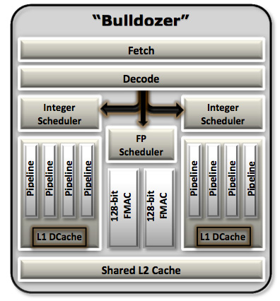
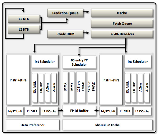
We'll start, logically, at the front end of a Bulldozer module. The fetch and decode logic in each module is shared by both integer cores. The role this logic plays is to fetch the next instruction in the thread being executed, decode the x86 instruction into AMD's own internal format, and pass the decoded instruction onto the scheduling hardware for execution.
AMD widened the K8 front end with Bulldozer. Each module is now able to fetch and decode up to four x86 instructions from a single thread in parallel. Each of the four decoders are equally capable. Remembering that each Bulldozer module appears as two cores, the front end can only pick 4 instructions to fetch and decode from a single thread at a time. A single Bulldozer module can switch between threads as often as every clock.
Decode hardware isn't very expensive on its own, but duplicating it four times across multiple cores quickly adds up. Although decode width has increased for a single core, multi-core Bulldozer configurations can actually be at a disadvantage compared to previous AMD architectures. Let's look at the table below to understand why:
| Front End Comparison | |||||
| AMD Phenom II | AMD FX | Intel Core i7 | |||
| Instruction Decode Width | 3-wide | 4-wide | 4-wide | ||
| Single Core Peak Decode Rate | 3 instructions | 4 instructions | 4 instructions | ||
| Dual Core Peak Decode Rate | 6 instructions | 4 instructions | 8 instructions | ||
| Quad Core Peak Decode Rate | 12 instructions | 8 instructions | 16 instructions | ||
| Six/Eight Core Peak Decode Rate | 18 instructions (6C) | 16 instructions | 24 instructions (6C) | ||
For a single instruction thread, Bulldozer offers more front end bandwidth than its predecessor. The front end is wider and just as capable so this makes sense. But note what happens when we scale up core count.
Since fetch and decode hardware is shared per module, and AMD counts each module as two cores, given an equivalent number of cores the old Phenom II actually offers a higher peak instruction fetch/decode rate than the FX. The theory is obviously that the situations where you're fetch/decode bound are infrequent enough to justify the sharing of hardware. AMD is correct for the most part. Many instructions can take multiple cycles to decode, and by switching between threads each cycle the pipelined front end hardware can be more efficiently utilized. It's only in unusually bursty situations where the front end can become a limit.
Compared to Intel's Core architecture however, AMD is at a disadvantage here. In the high-end offerings where Intel enables Hyper Threading, AMD has zero advantage as Intel can weave in instructions from two threads every clock. It's compared to the non-HT enabled Core CPUs that the advantage isn't so clear. Intel maintains a higher instantaneous decode bandwidth per clock, however overall decoder utilization could go down as a result of only being able to fill each fetch queue from a single thread.
After the decoders AMD enables certain operations to be fused together and treated as a single operation down the rest of the pipeline. This is similar to what Intel calls micro-ops fusion, a technology first introduced in its Banias CPU in 2003. Compare + branch, test + branch and some other operations can be fused together after decode in Bulldozer—effectively widening the execution back end of the CPU. This wasn't previously possible in Phenom II and obviously helps increase IPC.
A Decoupled Branch Predictor
AMD didn't disclose too much about the configuration of the branch predictor hardware in Bulldozer, but it is quick to point out one significant improvement: the branch predictor is now significantly decoupled from the processor's front end.
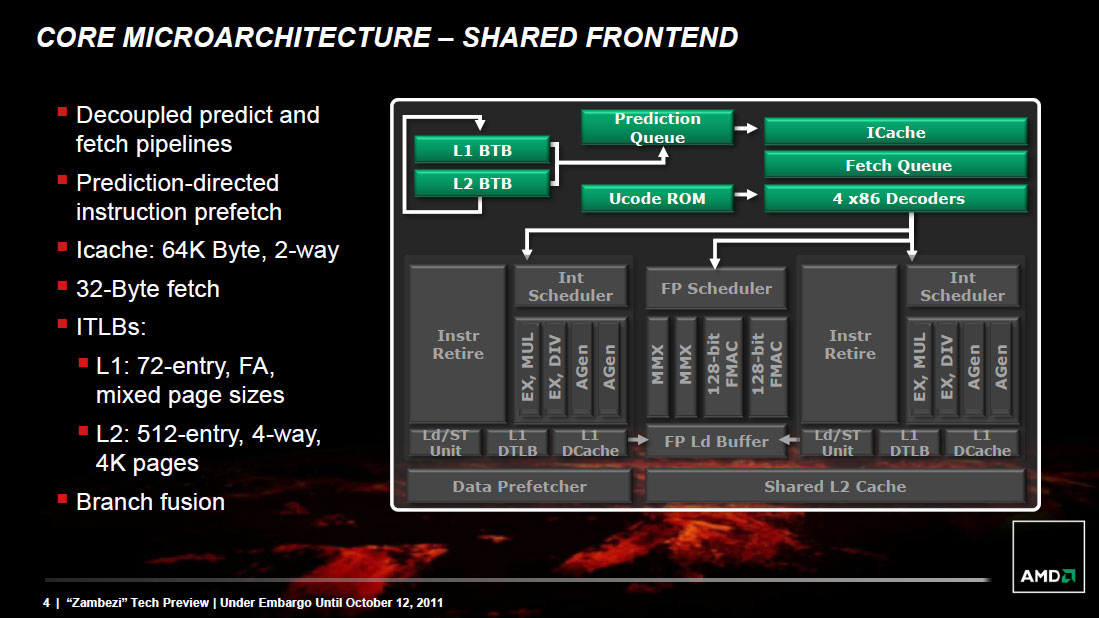
The role of the branch predictor is to intercept branch instructions and predict their target address, rather than allowing for tons of cycles to go by until the branch target is known for sure. Branches are predicted based on historical data. The more data you have, and the better your branch predictors are tuned to your workload, the more accurate your predictions can be. Accurate branch prediction is particularly important in architectures with deep pipelines as a mispredict causes more instructions to be flushed out of the pipe. Bulldozer introduces a significantly deeper pipeline than its predecessor (more on this later), and thus branch prediction improvements are necessary.
In both Phenom II and Bulldozer, branches are predicted in the front end of the pipe alongside the fetch hardware. In Phenom II however, any stall in the fetch pipeline (e.g. fetching an instruction that wasn't in cache) would stop the whole pipeline including future branch predictions. Bulldozer decouples the branch prediction hardware from the fetch pipeline by way of a prediction queue. If there's a stall in the fetch pipeline, Bulldozer's branch prediction hardware is allowed to run ahead and continue making future predictions until the prediction queue is full.
We'll get to the effectiveness of this approach shortly.
Scheduling and Execution Improvements
As with Sandy Bridge, AMD migrated to a physical register file architecture with Bulldozer. Data is now only stored in one location (the physical register file) and is tracked via pointers back to the PRF as operations make their way through the execution engine. This is a move to save power as copying data around a chip is hardly power efficient.
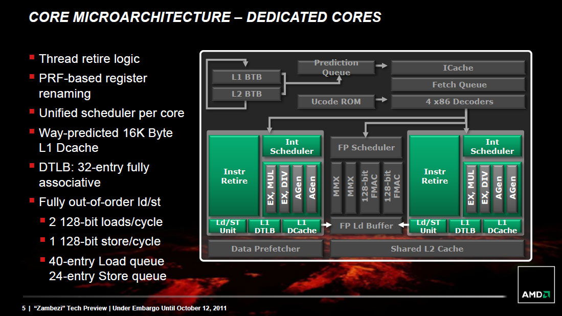
The buffers and queues that feed into the execution engines of the chip are all larger on Bulldozer than they were on Phenom II. Larger data structures allows for better instruction level parallelism when trying to execute operations out of order. In other words, the issue hardware in Bulldozer is beefier than its predecessor.
Unfortunately where AMD took one step forward in issue hardware, it does a bit of a shuffle when it comes to execution resources themselves. Let's start with the positive: Bulldozer's integer execution cores.
Integer Execution
Each Bulldozer module features two fully independent integer cores. Each core has its own integer scheduler, register file and 16KB L1 data cache. The integer schedulers are both larger than their counterparts in the Phenom II.
The biggest change here is each integer core now has two ports instead of three. A single integer core features two AGU/ALU ports, compared to three in the previous design. AMD claims the third ALU/AGU pair went mostly unused in Phenom II, and as a result it's been removed from Bulldozer.
With larger structures feeding into the integer cores, AMD should be able to have an easier time of making use of the integer units than in previous designs. AMD could, in theory, execute more integer operations per core in Phenom II however AMD claims the architecture was typically bound elsewhere.
The Shared FP Core
A single Bulldozer module has a single shared FP core for use by up to two threads. If there's only a single FP thread available, it is given full access to the FP execution hardware, otherwise the resources are shared between the two threads.
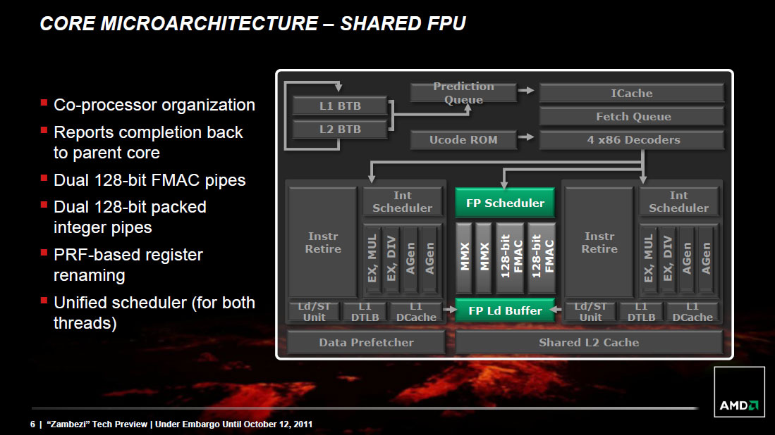
Compared to a quad-core Phenom II, AMD's eight-core (quad-module) FX sees no drop in floating point execution resources. AMD's architecture has always had independent scheduling for integer and floating point instructions, and we see the same number of execution ports between Phenom II cores and FX modules. Just as is the case with the integer cores, the shared FP core in a Bulldozer module has larger scheduling hardware in front of it than the FPU in Phenom II.
The problem is AMD had to increase the functionality of its FPU with the move to Bulldozer. The Phenom II architecture lacks SSE4 and AVX support, both of which were added in Bulldozer. Furthermore, AMD chose Bulldozer as the architecture to include support for fused multiply-add instructions (FMA). Enabling FMA support also increases the relative die area of the FPU. So while the throughput of Bulldozer's FPU hasn't increased over K8, its capabilities have. Unfortunately this means that peak FP throughput running x87/SSE2/3 workloads remains unchanged compared to the previous generation. Bulldozer will only be faster if newer SSE, AVX or FMA instructions are used, or if its clock speed is significantly higher than Phenom II.
Looking at our Cinebench 11.5 multithreaded workload we see the perfect example of this performance shuffle:
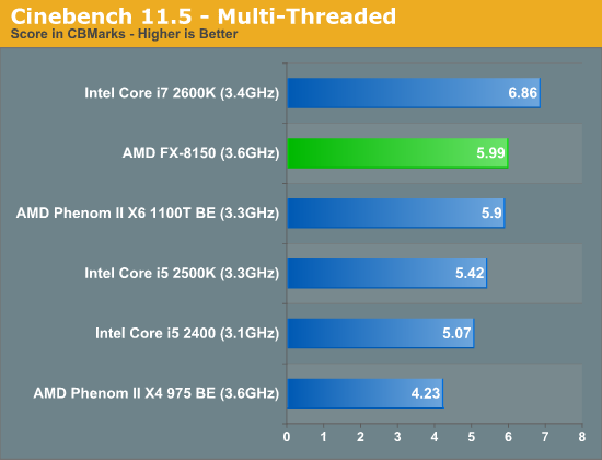
Despite a 9% higher base clock speed (more if you include turbo core), a 3.6GHz 8-core Bulldozer is only able to outperform a 3.3GHz 6-core Phenom II by less than 2%. Heavily threaded floating point workloads may not see huge gains on Bulldozer compared to their 6-core predecessors.
There's another issue. Bulldozer, at least at launch, won't have to simply outperform its quad-core predecessor. It will need to do better than a six-core Phenom II. In this comparison unfortunately, the Phenom II has the definite throughput advantage. The Phenom II X6 can execute 50% more SSE2/3 and x87 FP instructions than a Bulldozer based FX.
Since the release of the Phenom II X6, AMD's major advantage has been in heavily threaded workloads—particularly floating point workloads thanks to the sheer number of resources available per chip. Bulldozer actually takes a step back in this regard and as a result, you will see some of those same workloads perform worse, if not the same as the outgoing Phenom II X6.
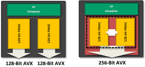
Compared to Sandy Bridge, Bulldozer only has two advantages in FP performance: FMA support and higher 128-bit AVX throughput. There's very little code available today that uses AMD's FMA instruction, while the 128-bit AVX advantage is tangible.
Cache Hierarchy and Memory Subsystem
Each integer core features its own dedicated L1 data cache. The shared FP core sends loads/stores through either of the integer cores, similar to how it works in Phenom II although there are two integer cores to deal with now instead of just one. Bulldozer enables fully out-of-order loads and stores, an improvement over Phenom II putting it on parity with current Intel architectures. The L1 instruction cache is shared by the entire bulldozer module, as is the L2 cache.
The instruction cache is a large 64KB 2-way set associative cache, similar in size to the Phenom II's L1 cache but obviously shared by more "cores". A four-core Phenom II would have 256KB of total L1 I-Cache, while a four core Bulldozer will have half of that. The L1 data caches are also significantly smaller than Bulldozer's predecessor. While Phenom II offered a 64KB L1 D-Cache per core, Bulldozer only offers 16KB per integer core.

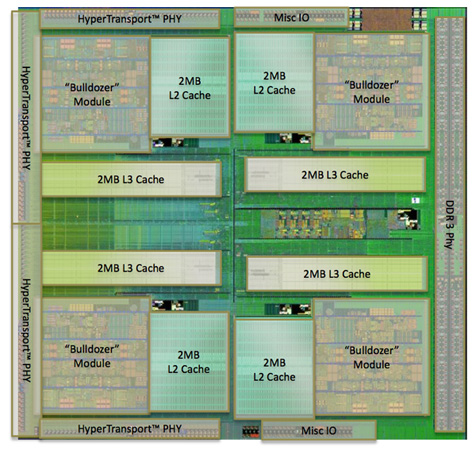
The L2 cache is much larger than what we saw in multi-core Phenom II designs however. Each Bulldozer module has a private 2MB L2 cache.
There's a single 8MB L3 cache that's shared among all Bulldozer modules on a chip. In its first incarnation, AMD has no plans to offer a desktop part without an L3 cache. However AMD indicated that the L3 cache was only really useful in server workloads and we might expect future Bulldozer derivatives (ahem, Trinity?) to forgo the L3 cache entirely as a result.
Cache accesses require more clocks in Bulldozer, due to a combination of size and AMD's desire to make Bulldozer a very high clock speed part...


430 Comments
View All Comments
medi01 - Thursday, October 13, 2011 - link
Slightest "problem" imaginable with AMD GPUs would make it into titles.nVidia article would go with comparing cherry picked overclocked board vs standard from AMD, with laughable "explanations" of "oh nVidia marketing asked us to do it, we kinda refused but then we thought that since we've already kinda refused, we might still do what they've asked".
"Objectively", are you kidding me?
JKflipflop98 - Thursday, October 13, 2011 - link
Anand runs the test, then writes down the number. Then he runs the test on the other PC, and writes down the number.If your number is lower, then it's physics "badmouthing" your precious, and not the site.
actionjksn - Wednesday, October 12, 2011 - link
@medi01 Considering the results I think Anand were more than kind enough to AMD.medi01 - Thursday, October 13, 2011 - link
I recall low power AMD CPUs being tested on 1000Watt PSUs on this very site. How normal was that, cough? iPhones "forgoten in pocket" (authors comment) on comparison photos where they would look unfavourably)Thing with tests is, you have games that favour one manufacturer, then other games that favour another. Choose "right" set of games, and viola...
The move with 1000Watt PSU on 35W TDP CPU is TOO DAMN LOW and should never happen.
On top of it, absolute majority of games is more GPU sensitive, than CPU sensitive. Now one could reduce resolution to ridiculously low levels so that CPU becomes a bottleneck. but then, who on earth would care whether you get 150 or 194 frames per second at a resolution which you'll never use?
Stas - Thursday, October 13, 2011 - link
Not sure what the deal is with PSUs or what article you're referring to. I'm assuming it made AMD power consumption look worse than it was because 1kW PSU was running at 10% load, thus way out of efficiency range. But w/e. My comment is mostly on CPU performance in games. Just because you don't run a game on the top-end CPU with $800 in multi-gpu tandem at lowest settings, doesn't mean it shouldn't be used to determine CPU performance. By making the CPU the bottleneck, you make it do as much as it can side-by-side with the GPU spiting out frames while whistling tunes and picking it's finger nails. There is more load on CPU than GPU. Which ever CPU is faster - that CPU will provide more FPS. Simple as that.Sure, no one will see 20%-30% performance difference using more appropriate resolution and quality settings. But we're enthusiasts, we want to see peak performance difference and extreme loads. Most synthetic tests are irrelevant in everyday use, but performance has been measured that way for decades.
jleach1 - Friday, October 14, 2011 - link
I haven't seen one single sentence that was questionable in a and graphics review. In fact I'm glad to say that I'm a big fan of Intel CPU and and hour combos, and have never had even as much as a hint of bias.As a over exaggeration, in an age where were all stuffing multiple cards in our systems, and cards are efficient, reliable, powerful, and they run cool. yes the drivers have sucked in the past, but they don't really.
(emphasis on the word seem)
NvIdia cards have just seemed clunky and hot as hell since the 400 series. I don't feel like gaming next to a space heater. And I definitely don't want to pay 40 percent more for ten percent performance just to have a space heater and bragging rights.
its like amd graphics are similar to intels CPU lineup, they're great performance per dollar parts, and they're efficient. But NvIdia and Intel graphics are like amd CPUs, they're either inefficient, or they're good at only a few things.
The moral? what the *$&* amd....you might as well write off the whole desktop business if the competition IS fifty percent faster and gaining ground....that 15 percent you're promising next year better be closer to 50 or I'm going to forget about your processors altogether.
jleach1 - Friday, October 14, 2011 - link
Intel CPU and amd combos*....sorry for the bat grammar. Writing on a tablet with Swype.CeriseCogburn - Wednesday, March 21, 2012 - link
40% more cost and 10% more performance?You said that's across the board.
I'm certainly glad you aren't the reviewer here on anything. I mean really that was over the top.
CeriseCogburn - Friday, June 8, 2012 - link
They went fullblown favor the bullsnoozer by using the GPU limited amd hd5870 to make the stupid amd cpu look good.Thank your lucky stars they did that much for you.
MJEvans - Thursday, October 13, 2011 - link
I think your later point is exactly why the FPU support isn't as strong. (most) tasks that use FPU appear to be operating on large matrices of data, while sequential processing seems to have a good design idea (even if the implementation is a little immature and a little early), but slower latency l1/l2 cache access. I hope that's an area that will be addressed by the next iteration.