Qualcomm's New Snapdragon S4: MSM8960 & Krait Architecture Explored
by Brian Klug & Anand Lal Shimpi on October 7, 2011 12:35 PM EST- Posted in
- Smartphones
- Snapdragon
- Arm
- Qualcomm
- Krait
- MDP
- Mobile
- SoCs
The Adreno 225 GPU
Qualcomm has historically been pretty silent about its GPU architectures. You'll notice that specific details of Adreno GPU execution resources have been absent from most of our SoC comparisons. Starting with MSM8960 however, this is starting to change.
The MSM8960 uses a current generation Adreno GPU with a couple of changes. Qualcomm calls this GPU the Adreno 225, a follow-on to Adreno 220. Subsequent Krait designs will use Adreno 3xx GPUs based on a brand new architecture.
As we discussed in our Samsung Galaxy S 2 review, Qualcomm's Adreno architecture is a tile based immediate mode renderer with early-z rejection. By Qualcomm's own admission, Adreno is somewhere in the middle of the rendering spectrum between IMRs and Imagination Technologies' TBDR architectures. One key difference is Adreno's tiling isn't as fine grained as IMG's.
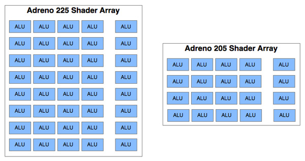
Architecturally the Adreno 225 and 220 are identical. Adreno 2xx is a DX9-class unified shader design. There's a ton of compute on-board with eight 4-wide vector units and eight scalar units. Each 4-wide vector unit is capable of a maximum of 8 MADs per clock, while each scalar unit is similarly capable of 2 MADs per clock. That works out to 160 floating point operations per clock, or 32 GFLOPS at 200MHz.
Update: Qualcomm has clarified the capabilities of its 4-wide Vector ALUs. Similar to the PowerVR SGX 543, each 4-wide vector ALU is capable of four MADs (one per component). The scalar units cannot be combined to do any MADs, although they are helpful we haven't really been tracking those in this table (IMG has something similar) so we've excluded them for now.
| Mobile SoC GPU Comparison | |||||||||||
| Adreno 225 | PowerVR SGX 540 | PowerVR SGX 543 | PowerVR SGX 543MP2 | Mali-400 MP4 | GeForce ULP | Kal-El GeForce | |||||
| SIMD Name | - | USSE | USSE2 | USSE2 | Core | Core | Core | ||||
| # of SIMDs | 8 | 4 | 4 | 8 | 4 + 1 | 8 | 12 | ||||
| MADs per SIMD | 4 | 2 | 4 | 4 | 4 / 2 | 1 | ? | ||||
| Total MADs | 32 | 8 | 16 | 32 | 18 | 8 | ? | ||||
| GFLOPS @ 200MHz | 12.8 GFLOPS | 3.2 GFLOPS | 6.4 GFLOPS | 12.8 GFLOPS | 7.2 GFLOPS | 3.2 GFLOPS | ? | ||||
| GFLOPS @ 300MHz | 19.2 GFLOPS | 4.8 GFLOPS | 9.6 GFLOPS | 19.2 GFLOPS | 10.8 GFLOPS | 4.8 GFLOPS | ? | ||||
Looking at the table above you'll see that this is the same amount of computing power than even IMG's PowerVR SGX 543MP2. However as we've already seen in our tests, Adreno 220 isn't anywhere near as quick.
Shader compiler efficiency and data requirements to actually populate a Vec4+1 array are both unknowns, and I suspect both significantly gate overall Adreno performance. There's also the fact that the Adreno 22x family only has two TMUs compared to four in the 543MP2, limiting texturing performance. Combine that with the fact that most Adreno 220 GPUs have been designed into single-channel memory controller systems and you've got a recipe for tons of compute potential limited by other bottlenecks.
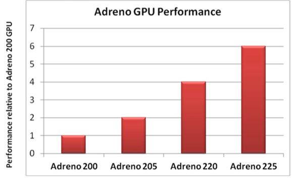
With Adreno 225 Qualcomm improves performance along two vectors, the first being clock speed. While Adreno 220 (used in the MSM8660) ran at 266MHz, Adreno 225 runs at 400MHz thanks to 28nm. Secondly, Qualcomm tells us Adreno 225 is accompanied by "significant driver improvements". Keeping in mind the sheer amount of compute potential of the Adreno 22x family, it only makes sense that driver improvements could unlock a lot of performance. Qualcomm expects the 225 to be 50% faster than the outgoing 220
Qualcomm claims that MSM8960 will be able to outperform Apple's A5 in GLBenchmark 2.x at qHD resolutions. We'll have to wait until we have shipping devices in hand to really put that claim to the test, but if true it's good news for Krait as the A5 continues to be the high end benchmark for mobile GPU performance.
While Adreno 225 is only Direct3D feature level 9_3 compliant, Qualcomm insisted that when the time is right it will have a D3D11 capable GPU using its own IP - putting to rest rumors of Qualcomm looking to license a third party GPU in order to be competitive in Windows 8 designs. Although Qualcomm committed to delivering D3D11 support, it didn't commit to a timeframe.


108 Comments
View All Comments
Blaster1618 - Saturday, October 8, 2011 - link
While Single instruction multiple data whether short or long vector is a great idea, sadly under utilized except in graphics processing, compressible signals and cryptography. Does the NEON technology just an additional graphics/compression engine? Does it require special Neon programming/compiling or does it enhance normal MIMD programming?happy medium - Sunday, October 9, 2011 - link
I thought the new tegra 3 was 5 cores?ET - Monday, October 10, 2011 - link
Thanks to Anandtech for covering mobile chips. I find it pretty exciting to read about these low power combinations of CPU and GPU.tech360 - Monday, October 10, 2011 - link
Excellent analysis. I guess x86 will have an uphill battle against ARM for years in bridging the gap in low power.Just wondering what are your thoughts on the integrated WiFi/GPS/BT/FM in S4? Does it have potential to integrate away the currently separate combo-chips?
Thanks.
The0ne - Monday, October 10, 2011 - link
I'm a fan of efficient coding and design and hope that Qualcomm is following that path. I think there's been too much "just get it done no matter what" in the programming business for far too long. That's not to say there aren't very good free open source apps out there by astounding programmers but the mainstream seems to have forgotten or don't care.This is good news because mobile is still in the early phases and if efficiency is priority things can only get better if not easier to debug, code, change, etc.
The bad is of course increasing speeds, any speeds like in the PC industry of yester-years. Sure we want more powerful hardware but lets not make it because of shotty code and design architectures. Again, in the mobile industry I believe these two points should be highly consider by anyone.
broccauley - Monday, October 10, 2011 - link
You need to add the ST-Ericsson Thor / NovaThor series of SoCs to your table.Also, of the SoCs in your table only the Qualcomm ones are true telecom SoCs - the others are mere application engines without telecom features.
ssiu - Tuesday, October 11, 2011 - link
Nothing about Apple A6? (I guess reliable info is hard to come by, but surely it would be out by December 2010 and should be included in the comparison table?)ssiu - Tuesday, October 11, 2011 - link
... December 2012 (where is the Edit button ...)sarge78 - Wednesday, October 12, 2011 - link
You could add the ZiiLabs ZMS-20 (and quad core ZMS-40) to the table. That'll probably see action in a Creative Android tablet/PMP and other OEMs might pick up the Jaguar reference tablet. (Could make a good review piece?)http://www.ziilabs.com/products/processors/zms20.a...
Or how about Marvell's 628 ARMADA tri-core SoC? Marvell are getting pushed out by Qualcomm but it could get some design wins next year (It has two 1.5GHz cores and a low power 624 MHz core, similar to Tegra 3)
http://www.marvell.com/company/news/pressDetail.do...
lancedal - Thursday, October 13, 2011 - link
Wouldn't the use of L0 impact performance?If L1 is shut-down, there will be penalty on a L0 miss. Powering up L1 on a L0 miss would cost thousand of cycles at 1.5GHz.
If L1 is on, then what is the point?