Qualcomm's New Snapdragon S4: MSM8960 & Krait Architecture Explored
by Brian Klug & Anand Lal Shimpi on October 7, 2011 12:35 PM EST- Posted in
- Smartphones
- Snapdragon
- Arm
- Qualcomm
- Krait
- MDP
- Mobile
- SoCs
Cache & Memory Hierarchy
Qualcomm has a three level exclusive cache hierarchy in Krait. The lower two levels are private per core, while the third level is shared among all cores. Qualcomm calls these caches L0, L1 and L2.
Each Krait core has an 8KB L0 cache (4KB instruction + 4KB data cache). The L0 cache is direct mapped and accessible in a single cycle. Qualcomm claims an 85% hit rate in this level 0 cache, which helps save power by not firing up the larger L1 cache. The hierarchy is exclusive so L0 data isn't necessarily duplicated in L1.
Each core also has a 32KB L1 cache (16KB instruction + 16KB data). The L1 4-way set associative and can also be accessed in a single cycle. There's no way prediction at work here. With 1 cycle latency to both L0 and L1, the primary advantage here is power.
| Krait Cache Architecture | |||||
| Size | Architecture | Frequency | |||
| L0 | 4KB + 4KB | Direct Mapped | Core | ||
| L1 | 16KB + 16KB | 4-way set associative | Core | ||
| L2 | 1MB (dual core) or 2MB (quad core) | 8-way set associative | 1.3GHz max | ||
The L2 cache is shared among all cores. In dual-core designs the L2 cache is sized at 1MB (up from 512KB in Scorpion), while quad-core Krait SoCs will have a 2MB L2. Krait's L2 cache is 8-way set associative.
While the L0 and L1 caches operate at core frequency and are on the same voltage plane as their associated core, the L2 cache is separate. To save power the L2 cache runs at its own frequency (up to 1.3GHz depending on the currently requested performance level). The L2 cache is on its own power plane and can be power gated if necessary.
Although Scorpion featured a dual-channel LPDDR2 memory controller, in a PoP configuration only one channel was available to any stacked DRAM. In order to get access to both 32-bit memory channels the OEM had to implement a DRAM on-package as well as an external DRAM on the PCB. Memory requests could be interleaved between the two DRAM, however Qualcomm seemed to prefer load balancing between the two with CPU/GPU accesses being directed to the lower latency PoP DRAM. Very few OEMs seemed to populate both channels and thus Scorpion based designs were effectively single-channel offerings.
Krait removes this limitation and now OEMs can utilize both memory channels in a PoP configuration (simply put two 32-bit DRAM die on the PoP stack) or in an external configuration. The split PoP/external DRAM organization is no longer supported. This change will hopefully mean we'll see more dual-channel Krait designs than we saw with Scorpion, which will in turn improve performance.
Process Technology and Clock Speeds
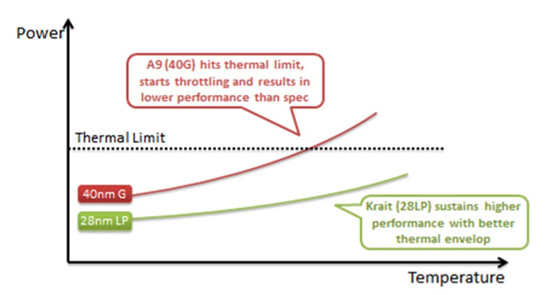
Krait will be the world's first smartphone CPU built on a 28nm process. Qualcomm is working with both TSMC and Global Foundries, although TSMC will produce the first chips. Krait will be built, at first, on TSMC's standard 28nm LP process. According to Qualcomm there's less risk associated with TSMC's non-HKMG process. Qualcomm was quick to point out that the entire MSM8960 SoC is built on a 28nm LP process compared to NVIDIA's 40nm LPG design in Kal-El. From Qualcomm's perspective, 40nm G transistors are only useful at reducing leakage at high temperatures but for the majority of the time a homogeneous LP design makes more sense.
Just like Scorpion, Krait places each core on its own voltage plane driven at its own clock frequency. Cores can be clocked independently of one another, which Qualcomm insists gives it a power advantage in many workloads.
The first implementation of Krait will be in a dual-core 1.5GHz MSM8960, however a second revision of the silicon will be introduced next year that increases clock speed to 1.7 - 2.0GHz. Qualcomm claims that at the same 1.05V core voltage, Krait can run at 1.7GHz vs. 1.55GHz for Scorpion. At these two clock speeds and at the same voltage, Qualcomm tells us that Krait consumes 265mW of power vs. 432mW running an undisclosed workload. Although it should be possible to draw more power than Scorpion under load, Krait should hopefully be able to improve overall power efficiency by completing tasks quicker and thus dropping down to idle faster than its predecessor. Smartphone and tablet battery life should remain the same at worst and improve at best, as a result.


108 Comments
View All Comments
skydrome1 - Monday, October 10, 2011 - link
I'm pretty sure they said it would sample by the end of this year and ship late 2012. If they were to delay it any more, they would be in serious trouble. ST Ericsson has quite a lot against them recently, and if they can't keep to their promises, TI is going to beat them quite badly. I'd estimate the Rogue to show up in an OMAP 5 in H2 2012 or H1 2013.All in all I'm just really excited by the PowerVR Rogue. Seeing the specifications of the Nova A9600 and what the Rogue can do is quite amazing. It's almost on par with the PS3.
Could an article on that be done once information is available?
I would love to have a portable gaming console :)
Haserath - Saturday, October 8, 2011 - link
Metafor is right about the curve having to do with the process. His explanation kinda makes it seem like a temp increase causes the power increase though. It's the power increase that causes the temp increase, and "G" transistors are designed to handle more power without wasted heat(temperature increase) compared to "LP" transistors. There's also a second reason why 28nm is hotter than 40nm.If you have a certain amount of heat energy being produced at a certain power level, the 40nm transistors will be a certain temperature.
Now take that same amount of heat energy being produced, and shrink the transistors to half their size. This increases their temperature within the same power envelope.
Of course they labeled a thermal limit on the power side, because the holder of whatever phone this chip goes into is going to feel the heat coming from the chip due to how much power it's using(how much heat energy is put out), not just due to the temperature of the transistors.
ViRGE - Saturday, October 8, 2011 - link
The graph is conceptually correct. While it's true that consuming more power produces more heat, the inverse is also true. The temperature of a transistor affects its leakage characteristics because resistance increases with heat. So at higher temperatures a CPU is going to consume more power to maintain its performance, compared to the same CPU at a lower temperature.You're basically looking at the principles of a superconductor applied in reverse.
JohnWH - Saturday, October 8, 2011 - link
The number of MADs per 4 way SIMD is 4 not 8 as stated (plus 1 for scalar channel), so total flops per clock is (4+1) * 2 * 8 = 80 flops/clock or 16GFLOPs/s @ 200MHz and 24GFlops/s @ 300MHz.Zingam - Saturday, October 8, 2011 - link
According to this article we'll have to wait for at least another 3 years or maybe more until we get tablets with enough power and good battery life that would be actually useful.Yeah, maybe at 14nm and with tri-gate transistors somewhen in 2016 we'll be able to enjoy true mobile computing all day long (at least 16 hours without a recharge).
Yeah, progress is good but way to slow sometimes. Too bad I was hoping for a ultracool and powerful e-book reader that delivers more tablet like experience rather than what currently is available.
dagamer34 - Saturday, October 8, 2011 - link
Define "useful". I'd argue that a lot of CPU cycles are wasted doing meaningless background tasks in apps that you can't see when it would be better to just pause and resume them later when the user brings them back into focus (aka Windows 8).bengildenstein - Saturday, October 8, 2011 - link
I'm trying to post a relevant comment but it's being flagged as spam. Can anyone offer any insight into why this may be the case?bengildenstein - Saturday, October 8, 2011 - link
The post centers around a siggraph 2011 talk that touches on Adreno 205's fragment shader performance.The gist is that the Adreno 205 (xperia play) showed faster performance with complex shaders than the SGX543MP2 (ipad2).
It seems I cannot post a link to the paper, but you can find it titled "Fast Mobile Shaders" at: aras-p [dot] info
Ryan Smith - Saturday, October 8, 2011 - link
The spam filter is pretty aggressive against links.http://www.aras-p.info/texts/files/FastMobileShade...
s44 - Saturday, October 8, 2011 - link
You sure it's the same Mali? I couldn't find it specified in any of Samsung's press releases.