Qualcomm's New Snapdragon S4: MSM8960 & Krait Architecture Explored
by Brian Klug & Anand Lal Shimpi on October 7, 2011 12:35 PM EST- Posted in
- Smartphones
- Snapdragon
- Arm
- Qualcomm
- Krait
- MDP
- Mobile
- SoCs
The Adreno 225 GPU
Qualcomm has historically been pretty silent about its GPU architectures. You'll notice that specific details of Adreno GPU execution resources have been absent from most of our SoC comparisons. Starting with MSM8960 however, this is starting to change.
The MSM8960 uses a current generation Adreno GPU with a couple of changes. Qualcomm calls this GPU the Adreno 225, a follow-on to Adreno 220. Subsequent Krait designs will use Adreno 3xx GPUs based on a brand new architecture.
As we discussed in our Samsung Galaxy S 2 review, Qualcomm's Adreno architecture is a tile based immediate mode renderer with early-z rejection. By Qualcomm's own admission, Adreno is somewhere in the middle of the rendering spectrum between IMRs and Imagination Technologies' TBDR architectures. One key difference is Adreno's tiling isn't as fine grained as IMG's.
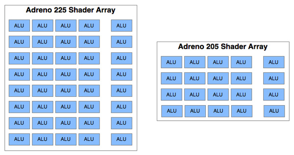
Architecturally the Adreno 225 and 220 are identical. Adreno 2xx is a DX9-class unified shader design. There's a ton of compute on-board with eight 4-wide vector units and eight scalar units. Each 4-wide vector unit is capable of a maximum of 8 MADs per clock, while each scalar unit is similarly capable of 2 MADs per clock. That works out to 160 floating point operations per clock, or 32 GFLOPS at 200MHz.
Update: Qualcomm has clarified the capabilities of its 4-wide Vector ALUs. Similar to the PowerVR SGX 543, each 4-wide vector ALU is capable of four MADs (one per component). The scalar units cannot be combined to do any MADs, although they are helpful we haven't really been tracking those in this table (IMG has something similar) so we've excluded them for now.
| Mobile SoC GPU Comparison | |||||||||||
| Adreno 225 | PowerVR SGX 540 | PowerVR SGX 543 | PowerVR SGX 543MP2 | Mali-400 MP4 | GeForce ULP | Kal-El GeForce | |||||
| SIMD Name | - | USSE | USSE2 | USSE2 | Core | Core | Core | ||||
| # of SIMDs | 8 | 4 | 4 | 8 | 4 + 1 | 8 | 12 | ||||
| MADs per SIMD | 4 | 2 | 4 | 4 | 4 / 2 | 1 | ? | ||||
| Total MADs | 32 | 8 | 16 | 32 | 18 | 8 | ? | ||||
| GFLOPS @ 200MHz | 12.8 GFLOPS | 3.2 GFLOPS | 6.4 GFLOPS | 12.8 GFLOPS | 7.2 GFLOPS | 3.2 GFLOPS | ? | ||||
| GFLOPS @ 300MHz | 19.2 GFLOPS | 4.8 GFLOPS | 9.6 GFLOPS | 19.2 GFLOPS | 10.8 GFLOPS | 4.8 GFLOPS | ? | ||||
Looking at the table above you'll see that this is the same amount of computing power than even IMG's PowerVR SGX 543MP2. However as we've already seen in our tests, Adreno 220 isn't anywhere near as quick.
Shader compiler efficiency and data requirements to actually populate a Vec4+1 array are both unknowns, and I suspect both significantly gate overall Adreno performance. There's also the fact that the Adreno 22x family only has two TMUs compared to four in the 543MP2, limiting texturing performance. Combine that with the fact that most Adreno 220 GPUs have been designed into single-channel memory controller systems and you've got a recipe for tons of compute potential limited by other bottlenecks.
With Adreno 225 Qualcomm improves performance along two vectors, the first being clock speed. While Adreno 220 (used in the MSM8660) ran at 266MHz, Adreno 225 runs at 400MHz thanks to 28nm. Secondly, Qualcomm tells us Adreno 225 is accompanied by "significant driver improvements". Keeping in mind the sheer amount of compute potential of the Adreno 22x family, it only makes sense that driver improvements could unlock a lot of performance. Qualcomm expects the 225 to be 50% faster than the outgoing 220
Qualcomm claims that MSM8960 will be able to outperform Apple's A5 in GLBenchmark 2.x at qHD resolutions. We'll have to wait until we have shipping devices in hand to really put that claim to the test, but if true it's good news for Krait as the A5 continues to be the high end benchmark for mobile GPU performance.
While Adreno 225 is only Direct3D feature level 9_3 compliant, Qualcomm insisted that when the time is right it will have a D3D11 capable GPU using its own IP - putting to rest rumors of Qualcomm looking to license a third party GPU in order to be competitive in Windows 8 designs. Although Qualcomm committed to delivering D3D11 support, it didn't commit to a timeframe.


108 Comments
View All Comments
metafor - Friday, October 7, 2011 - link
The SGX540 in the OMAP4460 is clocked significantly higher than (something TI is great at). So, while it isn't a powerhouse compared to Exynos or A5, it's more than sufficient. Google has never traditionally been top-of-the-line in terms of processors with their Nexus series. So it isn't out of the question they wouldn't be this time around either.dagamer34 - Saturday, October 8, 2011 - link
Technically, the Hummingbird SoC used in the Nexus S was top of the line at the time it was released (although it was eclipsed by dual-coe phones after 1-2 months). Also the Nexus One was the first major phone I can remember that had 512MB of RAM.However, it should be said that Google doesn't think about getting the best SoCs available for their product, but instead seeks to get the best deal on it's components from bidding against vendors. It's very possible that Samsung knows they had the most powerful SoC outside of the A5 and wanted Google to pay it for the value it would provide. Google instead apparently went with TI, likely because TI is selling it's chips cheaper in order to be the reference platform for Ice Cream Sandwich.
DanD85 - Friday, October 7, 2011 - link
Funny I saw Adreno 225 having 8 SIMDS and 5 MADS per SIMDS that should be equal to 40 total MADS right? Why it's 80? Am I missing sth?cptcolo - Friday, October 7, 2011 - link
Looking at the chart on "The Adreno 225 GPU" an comparing to the frame rates in the iPad 2 review (http://www.anandtech.com/show/4216/apple-ipad-2-gp... It looks like the PowerVR SGX543MP2 in the iPhone 4S will be about 33% faster. This is a very approximate estimate.cptcolo - Friday, October 7, 2011 - link
"Qualcomm claims that MSM8960 will be able to outperform Apple's A5 in GLBenchmark 2.x at qHD resolutions. We'll have to wait until we have shipping devices in hand to really put that claim to the test, but if true it's good news for Krait as the A5 continues to be the high end benchmark for mobile GPU performance."ssvb - Friday, October 7, 2011 - link
Please correct your CPU features comparison table (and in the previous articles too). ARM11 has a *pipelined* VFP, which actually makes it a lot faster than Cortex-A8 for double precision floating point workloads. You can have a look at the instruction cycle timings to get a better idea:ARM11 VFP - http://infocenter.arm.com/help/topic/com.arm.doc.d...
Cortex-A8 VFP - http://infocenter.arm.com/help/topic/com.arm.doc.d...
Thanks.
Anand Lal Shimpi - Friday, October 7, 2011 - link
Thank you! Fixed :)Take care,
Anand
icrf - Friday, October 7, 2011 - link
An ARM Cortext A9 has an 8 stage pipeline, not 9: http://www.arm.com/files/pdf/ARMCortexA-9Processor...Anand Lal Shimpi - Friday, October 7, 2011 - link
Thanks :)Take care,
Anand
Blaster1618 - Friday, October 7, 2011 - link
Maybe a noob, but I did not know that L0 memory could operate at GHz clock rate (5-10 times that of SD Ram clock rate. Good stuff, keep it coming. B-)