Apple Announces M1 Ultra: Combining Two M1 Maxes For Workstation Performance
by Ryan Smith on March 8, 2022 6:00 PM EST- Posted in
- SoCs
- Apple
- 2.5D
- Apple M1
- Apple M1 Max
- Apple M1 Ultra
As part of Apple’s spring “Peek Performance” product event this morning, Apple unveiled the fourth and final member of the M1 family of Apple Silicon SoCs, the M1 Ultra. Aimed squarely at desktops – specifically, Apple’s new Mac Studio – the M1 Ultra finds Apple once again upping the ante in terms of SoC performance for both CPU and GPU workloads. And in the process, Apple has thrown the industry a fresh curveball by not just combining two M1 Max dies into a single chip package, but by making the two dies present themselves as a single, monolithic GPU, marking yet another first for the chipmaking industry.
Back when Apple announced the M1 Pro and the ridiculously powerful M1 Max last fall, we figured Apple was done with M1 chips. After all, how would you even top a single 432mm2 chip that’s already pushing the limits of manufacturability on TSMC’s N5 process? Well, as the answer turns out to be, Apple can do one better. Or perhaps it would be more accurate to say twice as better. As for the company’s final and ultimate M1 chip design, the M1 Ultra, Apple has bonded two M1 Max dies together on to a single chip, with all of the performance benefits doubling their hardware would entail.
The net result is a chip that, without a doubt, manages to be one of the most interesting designs I’ve ever seen for a consumer SoC. As we’ll touch upon in our analysis, the M1 Ultra is not quite like any other consumer chip currently on the market. And while double die strategy benefits sprawling multi-threaded CPU and GPU workloads far more than it does more single-threaded tasks – an area where Apple is already starting to fall behind – in the process they re breaking new ground on the GPU front. By enabling the M1 Ultra’s two dies to transparently present themselves as a single GPU, Apple has kicked off a new technology race for placing multi-die GPUs in high-end consumer and workstation hardware.
M1 Max + M1 Max = M1 Ultra
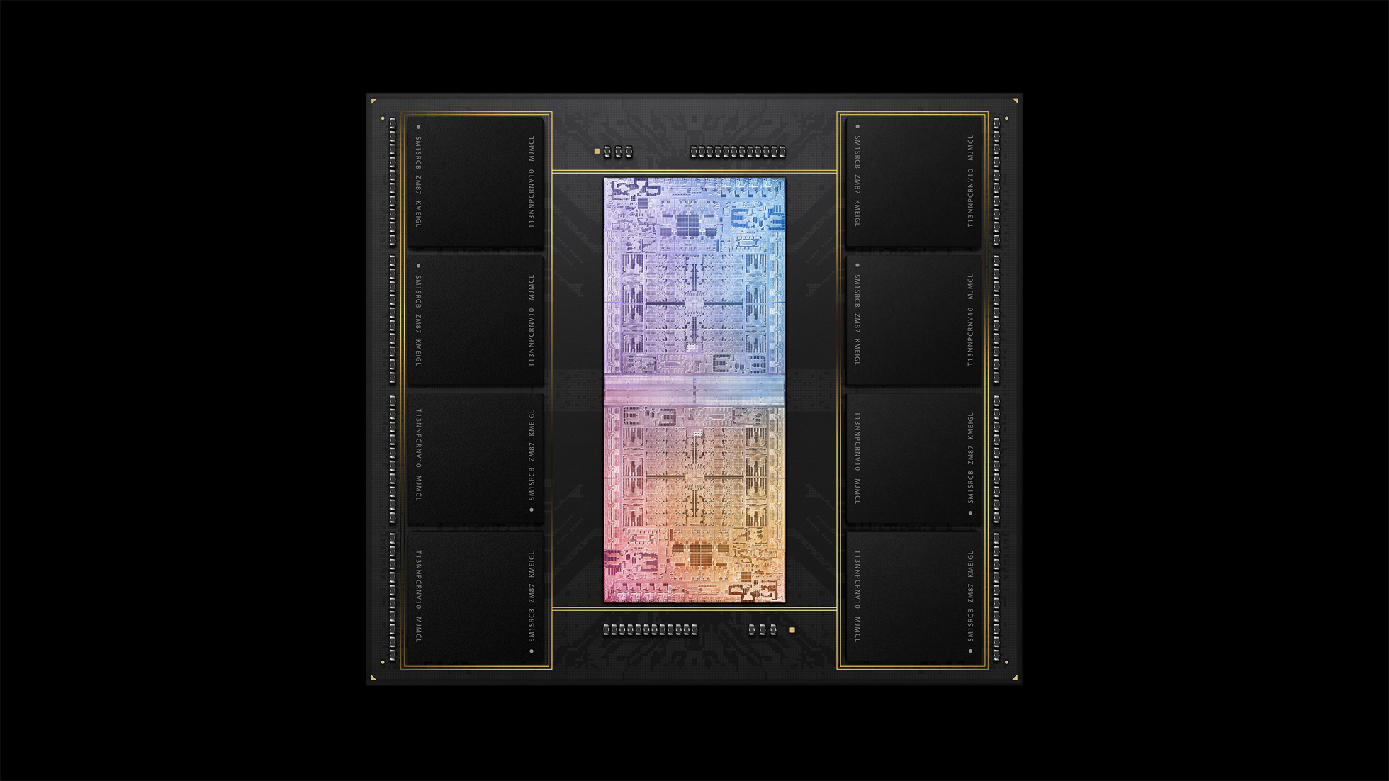
At the heart of the new M1 Ultra is something a bit older: the M1 Max. Specifically, Apple is using two M1 Max dies here, and then bonding them together to form a massive amalgamation of 114B transistors.
As M1 Max itself has been shipping for the last 5 months, the basic architecture of the chip (and its underlying blocks) is at this point a known quantity. M1 Ultra isn’t introducing anything new in teams of end-user features in that respect, and instead the chip is all about scaling up Apple’s M1 architecture one step further by placing a second silicon die on a single chip.
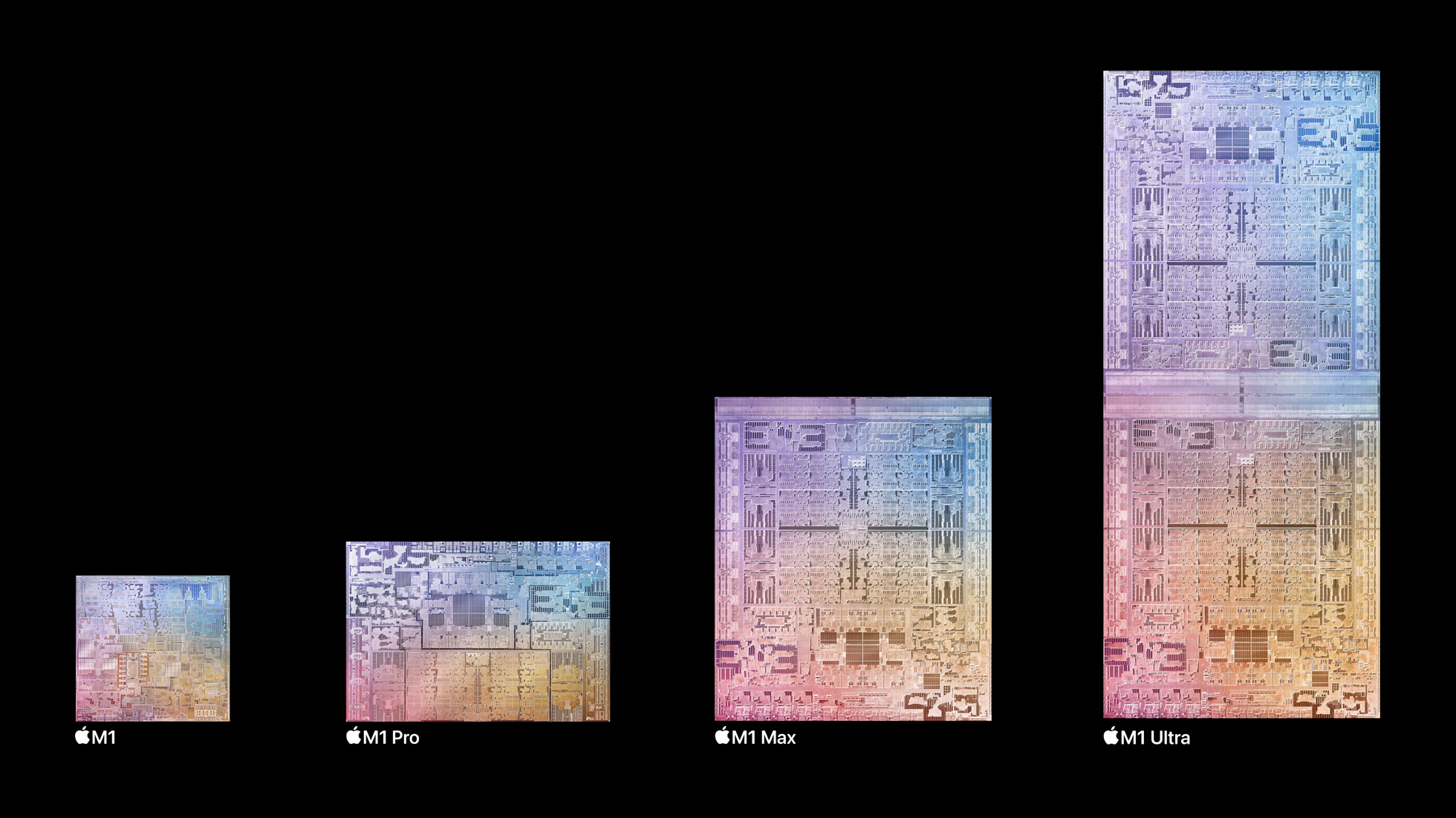
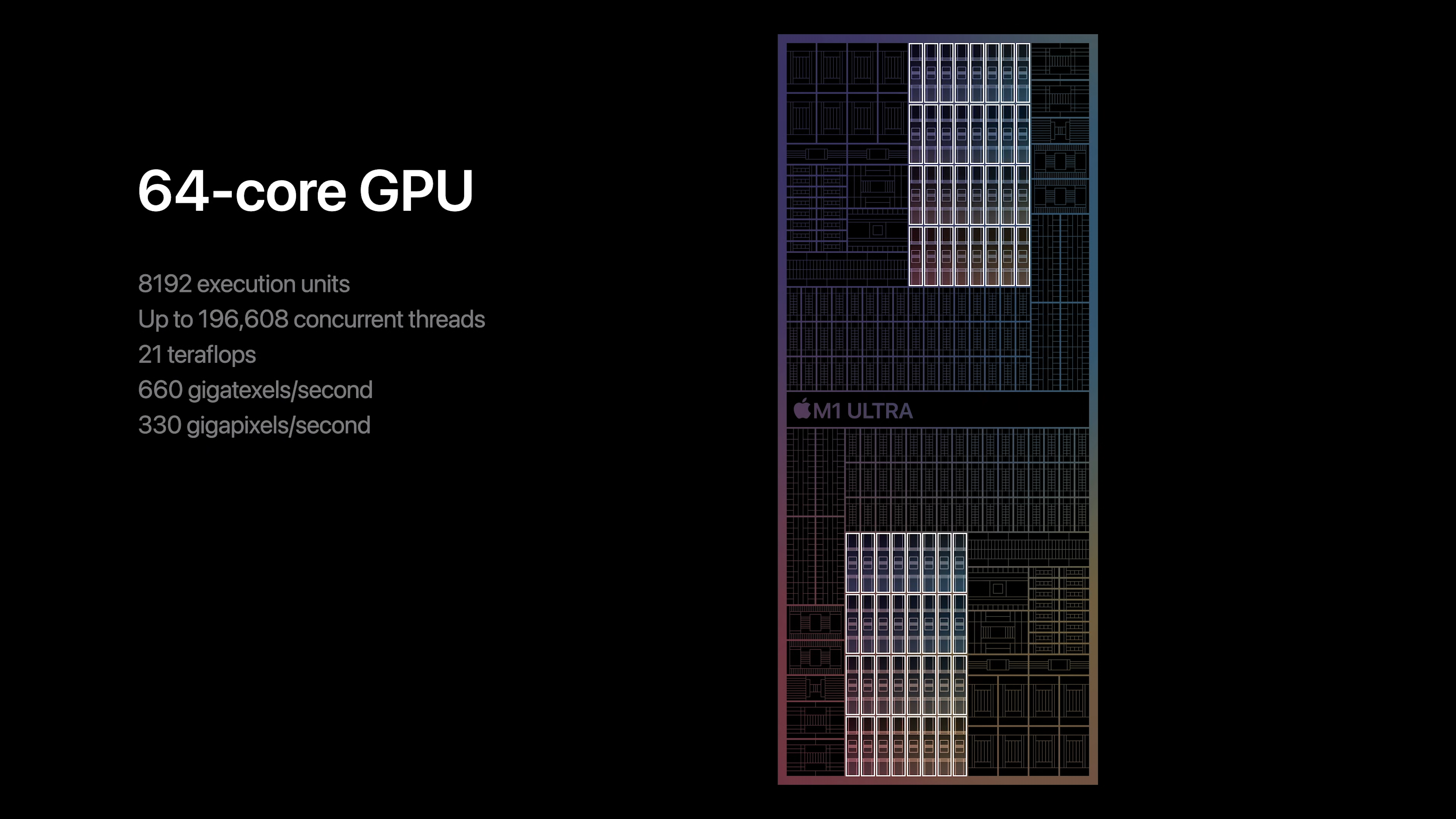
Starting with speeds and feeds, by placing two M1 Max dies on a single package, Apple has doubled the amount of hardware at their disposal in virtually every fashion. This means twice as many CPU cores, twice as many GPU cores, twice as many neural engine cores, twice as many LPDDR5 memory channels, and twice as much I/O for peripherals.
On the CPU front, this means Apple now offers a total of 20 CPU cores. This is comprised of 16 of their performance-focused Firestorm cores, and 4 of their efficiency-focused Icestorm cores. Given that M1 Ultra is aimed solely at desktops (unlike M1 Max) the efficiency cores don’t have quite as big of a role to play here since Apple doesn’t need to conserve energy down to the last joule. Still, as we’ve seen they’re fairly potent cores on their own, and will help add to the CPU throughput of the chip in heavily threaded scenarios.
As is typical for an Apple product announcement, the company isn’t disclosing clockspeeds here. The desktop-focused nature of the chip means that, if they desire, Apple can push clockspeeds a bit higher than they did on the M1 Max, but they would need to leave their energy efficiency sweet spot to do it.
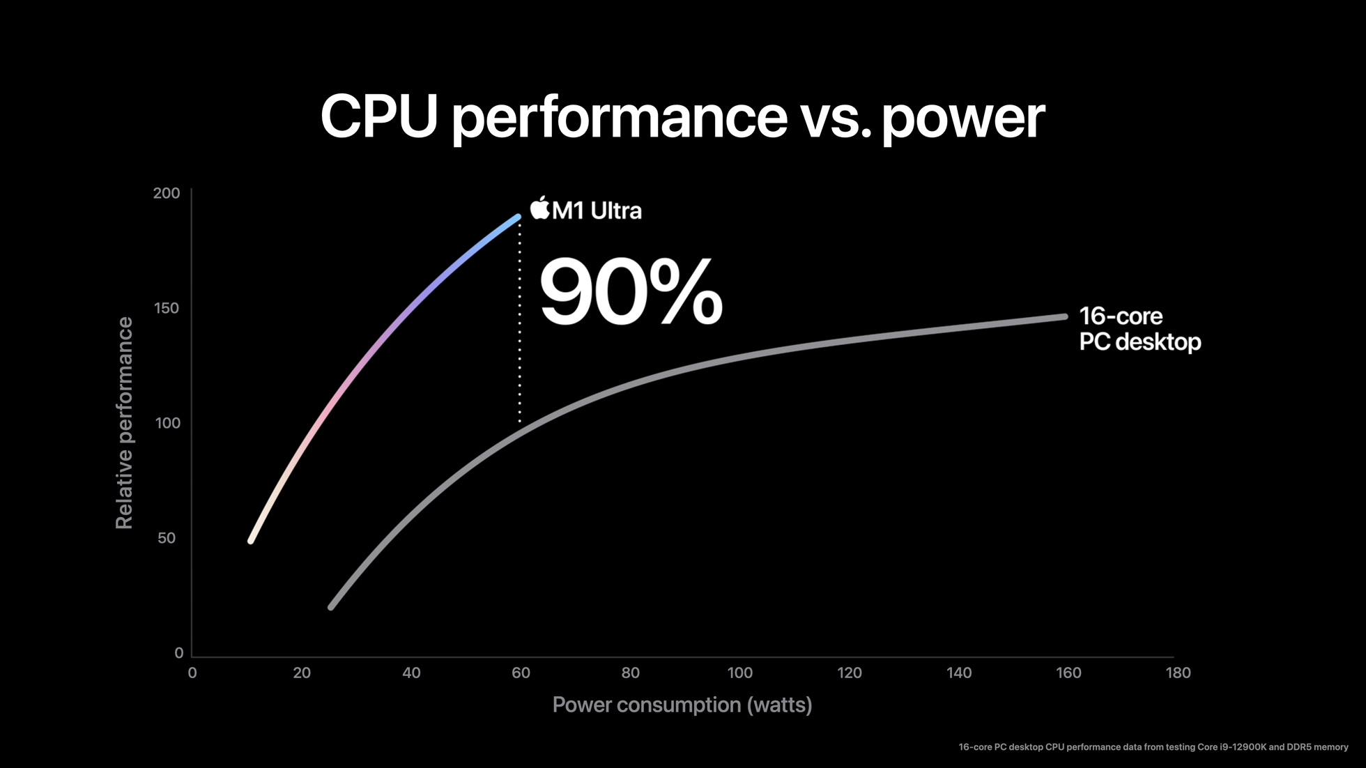
In practice, I will be surprised if the M1 Ultra CPU cores are clocked much higher than on the M1 Max. Which for Apple’s CPU performance is mixed blessings. For multithreaded workloads, 16 Firestorm cores is going to provide enough throughput to top some performance charts. But for single/lightly-threaded workloads, Firestorm has already been outpaced by newer architectures such as Intel’s Golden Cove CPU architecture. So don’t expect to see Apple recover the lead for single-threaded performance here; instead it’s all about MT and especially energy efficiency.
Meanwhile, doubling the number of M1 Max dies on the chip means that Apple is able to double the number of memory channels on the chip, and thus their overall memory bandwidth. Whereas M1 Max had 16 LPDDR5-6400 channels for a total of 408GB/second of memory bandwidth, M1 Ultra doubles that to 32 LPDDR5 channels and 800GB/second of memory bandwidth. And as with the M1 Max, this is accomplished by soldering the LPDDR5 chips directly to the chip package, for a total of 8 chips on M1 Ultra.
The doubled memory chips also allows Apple to double the total amount of memory available in their hardware. Whereas M1 Max topped out at 64GB, M1 Ultra tops out at 128GB. This is still less memory than could be found on a true high-end workstation (such as a Mac Pro), but it puts Apple ahead of all but the highest-end PC desktops, and should be plenty sufficient for their content creator crowd.
As we saw with the launch of the M1 Max, Apple already provides more bandwidth to their SoCs than the CPU cores alone can consume, so the doubled bandwidth isn’t likely to have much of an impact there than otherwise ensuring that the CPU cores are just as well fed as they are on the M1 Max. Instead, all of this extra memory bandwidth is meant to keep pace with the growing number of GPU cores.
Which brings us to the most interesting aspect of the M1 Ultra: the GPU. With 32 GPU cores, M1 Max was already setting records for a monolithic, integrated GPU. And now Apple has doubled things to 64 GPU cores on a single chip.
Unlike multi-die/multi-chip CPU configurations, which have been commonplace in workstations for decades, multi-die GPU configurations are a far different beast. The amount of internal bandwidth GPUs consume, which for high-end parts is well over 1TB/second, has always made linking them up technologically prohibitive. As a result, in a traditional multi-GPU system (such as the Mac Pro), each GPU is presented as a separate device to the system, and it’s up to software vendors to find innovative ways to use them together. In practice, this has meant having multiple GPUs work on different tasks, as the lack of bandwidth meant they can’t effectively work together on a single graphics task.
But, if you could somehow link up multiple GPUs with a ridiculous amount die-to-die bandwidth – enough to replicate their internal bandwidth – then you might just be able to use them together in a single task. This has made combining multiple GPUs in a transparent fashion something of a holy grail of multi-GPU design. It’s a problem that multiple companies have been working on for over a decade, and it would seem that Apple is charting new ground by being the first company to pull it off.
UltraFusion: Apple’s Take On 2.5 Chip Packaging
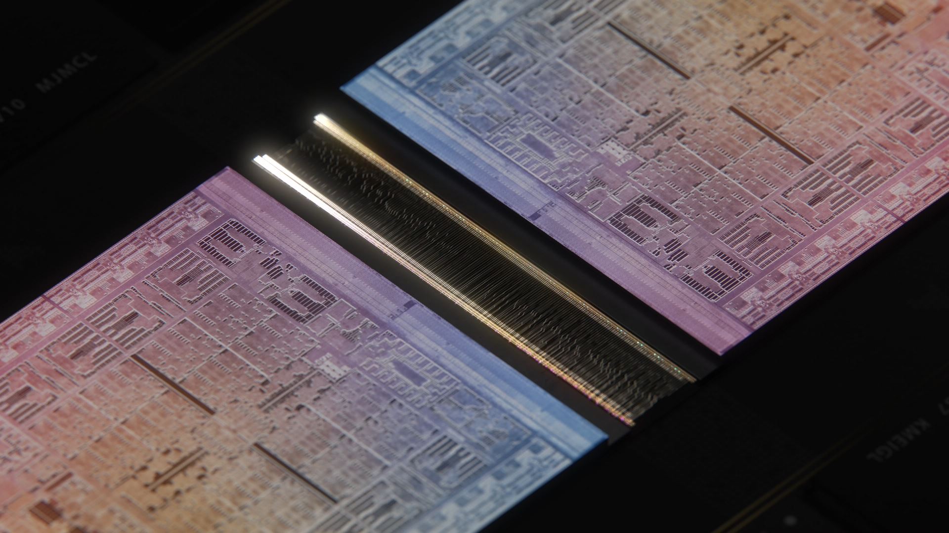
The secret ingredient that makes this all possible – and which Apple has been keeping under wraps until today – is that M1 Max has a very high speed interface along one of its edges. An interface that, with the help of a silicon interposer, allows two M1 Max dies to be linked up.
Apple calls this packaging architecture UltraFusion, and it’s the latest example in the industry of 2.5D chip packaging. While the details very from implementation to implementation, the fundamentals of the technology are the same. In all cases, some kind of silicon interposer is put beneath two chips, and then signals between the two chips are routed through the interposer. The ultra-fine manufacturing capabilities of silicon mean that an enormous number of traces can be routed between the two chips – in Apple’s case, over 10,000 – which allows for an ultra-wide, ultra-high bandwidth connection between the two chips.
Officially, Apple only states they’re using a silicon interposer here, which is the generic term for this technology. But, going by Apple’s promotional videos and mockup animations, it looks like they’re using a small, silicon bridge of some sort. Which would make this similar in implementation to Intel’s EMIB technology or Elevated Fanout Bridge (EFB) technology. Both of these are already on the market and have been used for years, so Apple is far from the first vendor to use the technology. But what they’re using it for is quite interesting.
With UltraFusion, Apple is able to offer an incredible 2.5TB/second of bandwidth between the two M1 Max dies. Even if we assume that this is an aggregate figure – adding up both directions at once – that would still mean that they have 1.25TB/second of bandwidth in each direction. All of which is approaching how much internal bandwidth some chips use, and exceeds Apple’s aggregate DRAM bandwidth of 800GB/second.
We’ll go more into this in the obligatory follow-up article, but the important point to take away here is that Apple has become the first vendor to bond two GPUs together with such a massive amount of bandwidth. This is what’s enabling them to take a stab at presenting the two GPUs as a single device to the OS and applications, as it allows them to quickly shuffle data between the GPUs as necessary.
But it should also be noted that there are plenty of details that can make or break the usefulness of this approach. For example, is 2.5TB/second enough, given the high performance of the GPUs? And what is the performance impact of the additional latency in going from GPU to GPU? Just because Apple has doubled the number of GPU cores by gluing them together doesn’t mean Apple has doubled their GPU performance. But at the end of the day, if it works even remotely well, then the implications for GPU designs going forward are going to be immense.
GPU Performance: Exceeding GeForce RTX 3090
Thanks to UltraFusion, Apple has become the first vendor to ship a chip that transparently combines two otherwise separate GPUs. And while we’ll have to wait for reviews to find out just how well this works in the real world, Apple is understandably excited about their accomplishment, and the performance implication thereof.
In particular, the company is touting that the M1 Ultra’s GPU performance exceeds that of NVIDIA’s GeForce RTX 3090, which at the moment is the single fastest video card on the market. And furthermore, that they’re able to do so while consuming a bit over 100 Watts, or 200 Watts less than the RTX 3090.
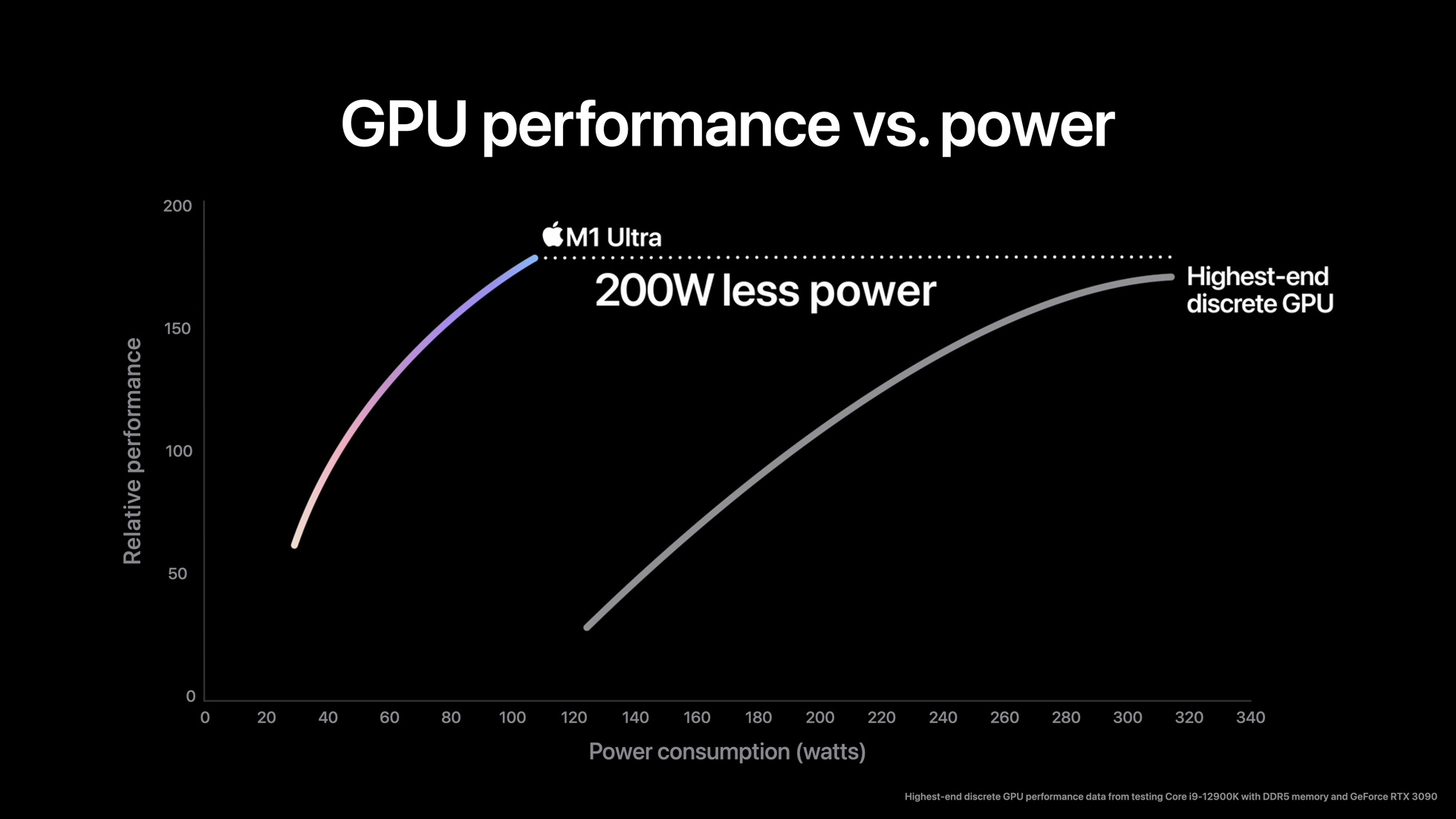
From a performance standpoint, Apple’s claims look reasonable, assuming their multi-GPU technology works as advertised. For as fast as the RTX 3090 is, it can’t be overstated just how many more transistors Apple is throwing at the matter than NVIDIA is; the GA102 GPU used by NVIDIA has 28.3 billion transistors, while the combined M1 Ultra is 114 billion. Not all of which are being used for graphics on the M1 Ultra, of course, but with so many transistors, Apple doesn’t have to be shy about throwing more silicon at the problem.
The amount of silicon Apple has at their disposal is also one of the keys to their low power consumption. As we’ve already seen with the M1 Max, Apple has built a wide enough GPU that they can keep clockspeeds nice and low on the voltage/frequency curve, which keeps overall power consumption down. The RTX 3090, by contrast, is designed to chase performance with no regard to power consumption, allowing NVIDIA to get great performance out of it, but only by riding high on the voltage frequency curve. And of course, Apple enjoys a huge manufacturing process advantage here, using TSMC’s N5 process versus Samsung’s 8nm process.
Still, given the ground-breaking nature of what Apple is trying to pull off with their transparent multi-GPU design, it has to be emphasized that Apple’s performance claims should be taken with a grain of salt, at least for now. Apple typically doesn’t do things half-baked, but as combining two GPUs in this fashion is yet unproven, a bit of skepticism is healthy here.
First Thoughts
While Apple has telegraphed their intention to scale up their chip designs since the first days of their Apple Silicon-powered Macs, I believe it’s safe to say that the M1 Ultra exceeds most expectations. Having reached the practical limits of how big they can make a single die, Apple has taken the logical next step and started placing multiple dies on a single chip in order to build a workstation-class processor. A step that is necessary, given the constraints, but also a step that is historically more cutting edge than is typical even for Apple.

The net result is that Apple has announced a SoC that has no peer in the industry across multiple levels. Going multi-die/multi-chip in a workstation is a tried and true strategy for CPUs, but to do so with GPUs will potentially put Apple on a level all of their own. If their transparent multi-GPU technology works as well as the company claims, then Apple is going to be even farther ahead of their competitors both in performance and in developing the cutting-edge technologies needed to build such a chip. In that respect, while Apple is trailing the industry a bit with their UltraFusion 2.5D chip packing technology, what they’re attempting to do with it is more than making up for lost time.
All of which is to say that we’re very eager to see how M1 Ultra performs in the real world. Apple has already set a rather high bar with the M1 Max, and now they’re aiming to exceed it with the M1 Ultra. And if they can deliver on those goals, then they will have twice set a new high point for SoC design in the span of just 6 months. These are exciting times, indeed.


219 Comments
View All Comments
Tomatotech - Monday, March 14, 2022 - link
Thanks for the clarification. That phrase 'We're adding one last chip to the M1 family' wasn't in the AnandTech liveblog, but Ars Technica reported it in their liveblog.That's interesting, because speculation is that the Mac Pro will have 2x M1 Ultras glued together - that lines up with all the previous rumours about the new Mac Pro's upcoming capabilities. But every time Apple have stuck two chips together, they've given it a new name. M1 Ultra = 2x M1 Max = 4x M1 Pro.
So either this is NOT the final (and apple didn't use the word 'final') M1 chip, OR it will be called the M2 (unlikely) OR it will be 2x M1 Ultra chips in separate packages, not connected together.
Using 2 separate packages seems un-Apple like, and introduces unnecessary complexity / issues. So my money is on the first option - that Apple will introduce yet another M1 variant for the Mac Pro. "We said in March that we were adding one last chip, the M1 Ultra. Well, guess what, we've made a new one! Witness the M1 <Plaid>!"
Historical evidence:
(1) Apple constantly one-upping themselves each year.
(2) M1 Max being inferior (!) to the later release of the M1 Ultra.
michael2k - Tuesday, March 15, 2022 - link
Connecting two M1 Ultra is no more complex than connecting two GPUs in the current Mac Pro. At the worst they use PCIe5 x16 for 128GB/s between chips and at best they use UCIe and if they can keep the two chips 2mm apart they can connect them at 1.2TB/sandynormancx - Tuesday, March 15, 2022 - link
It seems far more likely to me, as already discussed here, that they’ll wait for the M2 for the Pro and that the M2 will have extra interconnects to allow them to combine more than 2 dies at a time.That might be a struggle within their original migration target, but it is entirely possible that they might pre announce the new Pro sometime before it is available, giving them a bit more time.
involuntarheely - Tuesday, March 15, 2022 - link
that's very unlikely because Apple will never give up scale economies for M2. they obviously went this path with the M1. they started with iphone and by the time the A13 (or whatever the number was) became M1 they had produced millions and brought production costs down. then they came up with M1pro/max when those became cheap to make. and so on.they will introduce the M2 on Air/mini, then MBP 14/16, then iMac, then Studio, then Pro, which I'm guessing follows the sales numbers of the respective devices (save for the mini, I guess).
there would be a huge cost in starting M2 sales with the Pro.
BillBear - Wednesday, March 16, 2022 - link
It's also possible that the chips in the Mac Pro line will be considered a different chip family altogether.One that focuses on throughput without caring about power draw or production costs.
I wouldn't be surprised to see massive amounts of HBM,for example, that would not be cost effective in a consumer product like an iPad, but is already in use in high end products from others.
Bevans868 - Saturday, March 12, 2022 - link
Is it possible that synthetic benchmarks are currently capable of accurately Apple SOC chip architecture? When you add encoders/decoders, unified memory, neural engines I think they underestimate real workloads.brucethemoose - Tuesday, March 15, 2022 - link
Well that goes both ways if you, for instance, start talking about nvenc and CUDA. Or the ASICs in the AMD consoles.The M1 series is very good at media processing though, I don'f think anyone will dispute that.
Mehen - Monday, March 14, 2022 - link
Either Apple does not know how to label a graph properly, or I think there are some major misinterpretations going on here.The GPU performance vs. power graph.
Y-Axis = "Relative Performance."
Not "Performance." It says "Relative Performance."
Relative to what? It's clearly not relative to the 3090 setup (otherwise the 3090 results don't make sense, it would have to be a straight horizontal line). From how I read it, "Relative Performance" is "Performance / Watt." Let's call it P/W. You can think of P as Performance Points, kind of like a 3D mark score or something.
Let's look at the maximum performance on the graph. The top of the M1 Ultra looks to hit about 108W (just a little below the midpoint between 100 and 120 on the X-Axis).
So at 108W, the M1 Ultra hits ~180 on Relative Performance (P/W).
So 180P/W x 108W = 19,440 Points.
The highest point of the 3090 setup is about 315W. The way the graph reads, I'd peg this around 170P/W, but lets use the 90% figure they also used on the CPU graph, and give the Apple chip even more of a lead, (180P/W x .90) and we get 162P/W for the 3090 setup.
So at 315W, the 3090 set up is ~162 on Relative Performance (P/W).
So 162P/W x 315W = 51,030 Points. (It would be even more if I used 170P/W)
So the M1 Ultra is still very impressive, scoring about 38% of the 3090 setup (19,440 / 51,030), at only 34% of the power (108W / 315W).
Of course, if they actually provided some sort of units or benchmarks for the Y-Axis, they could clarify this whole mess of a graph. If it really is that fast, label is properly!
Don't these numbers seem much more reasonable? And it seems to fit better with how previous chips compare with low TDP versions of the graphics cards (mobile 3080's for example).
Thoughts? I feel like Apple is intentionally misleading us with that "200W less power" notation.
bifford - Monday, March 14, 2022 - link
"Relative performance" does not mean performance per watt. "Relative performance" just means that the ratios between the two chips are accurate but it does not have a specific unit. This is very common nomenclature in science when comparing two processes. It is probably based on a summary of their internal benchmarking process scaled to make the numbers pretty.Mehen - Monday, March 14, 2022 - link
Gotcha. The scaling thing makes sense, I think that is what I was missing. And... well... I guess my next gaming rig is going to be a Mac then!