Marvell Announces OCTEON 10 DPU Family: First to 5nm with N2 CPUs
by Andrei Frumusanu on June 28, 2021 6:30 AM EST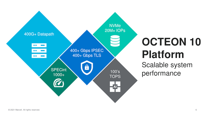
It’s been a little over a year since we covered Marvell’s OCTEON TX2 infrastructure processors, and since then, the ecosystem has been evolving in an extremely fast manner – both within Marvell and outside. Today, we’re covering the new generation OCTEON 10 family of DPUs, a whole new family of SoCs, built upon TSMC’s 5nm process node and also for the featuring for the first time Arm’s new Neoverse N2 processors.
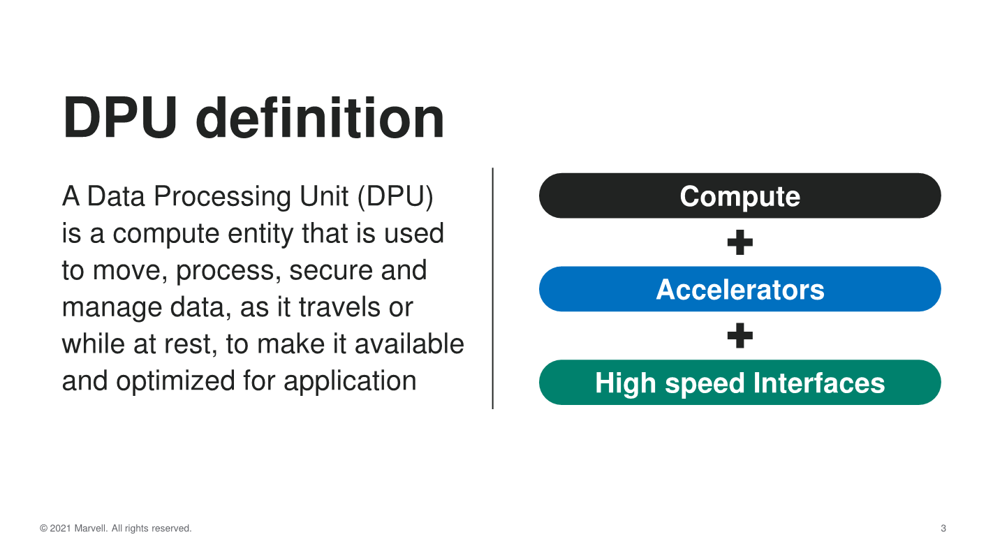
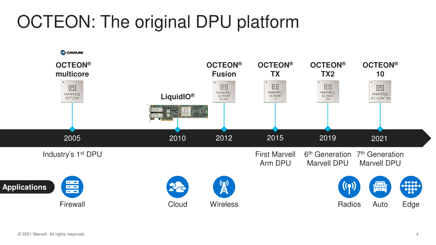
Starting off with a bit of history and nomenclature, Marvell is adopting the “DPU” term for this class of chip and accelerator type. The previous generation OCTEON TX and OCTEON TX2 already were DPUs in everything but name, previously simply being referenced as “infrastructure processors”. With the recent industry rising popularity of the term as well as competitor solutions being propped up, it seems we’re seeing the DPU term now being widely accepted nomenclature for this type of versatile chip design, defined by the fact that it’s an entity that helps process and move data while it travels through the network.
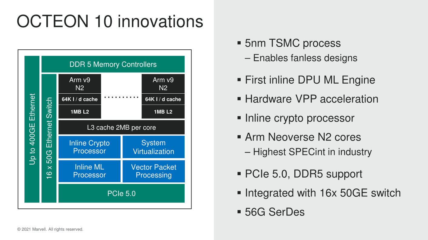
Starting with an overview, the new OCTEON 10 generally features the same versatile array of building blocks we’ve seen in the previous generation, this time upgraded to the new state of the art IP blocks, and also introducing some new features such as integrated machine learning inference engine, new inline and crypto processors as well as vector packet processors, all able to operated in a virtualised manner.
This is also Marvell’s first TSMC N5P silicon design, actually the first DPU of its kind on the new process, and also the first publicly announced Neoverse N2 implementation, featuring the newest PCIe 5.0 I/O capabilities as well as DDR5 support.

Starting off with what Marvell views as an important addition to the DPU, is a new in-house ML engine. Marvell had stated that the design for the IP had actually been originally created for a dedicated inference accelerator, and actually had been completed last year, but with Marvell opting to not bring it to market due to the extremely crowded competitive landscape. Instead, Marvell has opted to integrate the ML accelerator into their OCTEON DPU chips. Marvell here states that having the inference accelerator on the same monolithic silicon chip, directly integrated into the data pipeline is extremely important in achieving the low latency for higher throughput processing required for these kinds of data stream use-cases.
Essentially Marvell here is offering a competitor solution to Nvidia’s next-gen BlueField-3 DPU in terms of AI processing capabilities well ahead in terms of product generation, as the first OCTEON 10 solutions are expected to be sampling by end of this year while Nvidia projected BF3 to be arriving in 2022.
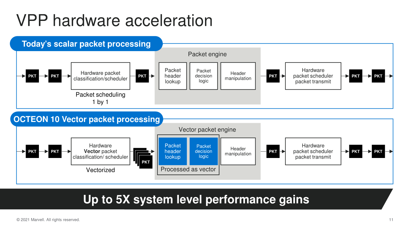
Also, a new capability of the new OCTEON 10 family is the introduction of vector packet processing engines, which are able to vastly augment the packet processing throughput by a factor of 5x compared to the current generation scalar processing engines.
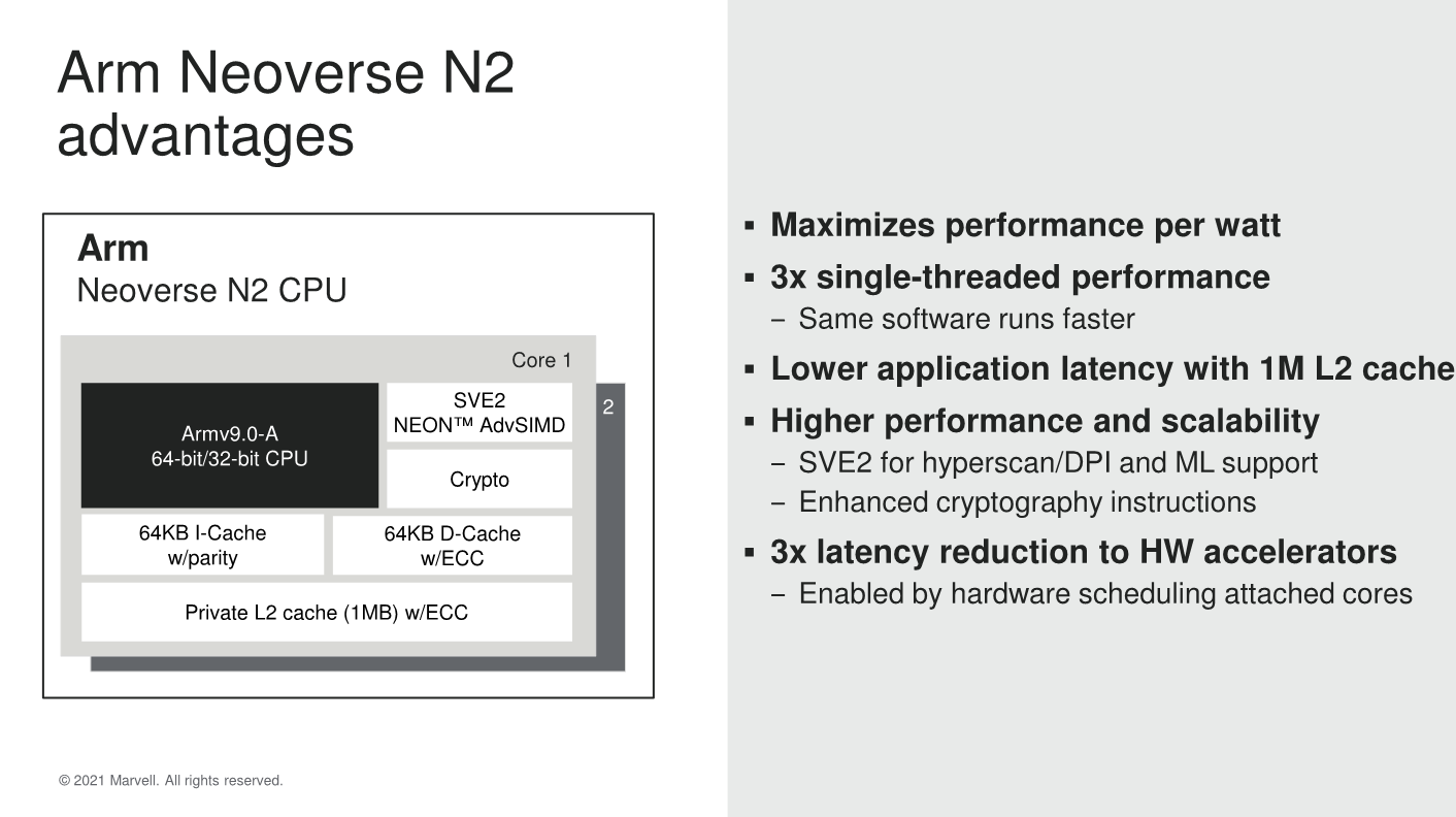
As noted, the new OCTEON 10 DPU family is the first publicly announced silicon design featuring Arm’s newest Neoverse N2 infrastructure CPU IP. We had covered the N2 and its HPC V1 sibling a couple of months ago – the jist of it is that the new generation core is the first Armv9 core from Arm and promises large 40% IPC gains in comparison to the current N1 core seen in Arm server CPUs such as the Amazon Graviton2 or Ampere Altra.
For Marvell, the performance improvements are even more significant as the company is switching over from the company’s previous in-house “TX2” CPU IP for the N2 core, promising a massive 3x higher single-threaded performance uplift. Late last year, Marvell had announced that it had stopped its own CPU IP in favour of Arm’s Neoverse cores, and today reiterated that the company is planning to stick to Arm’s roadmap for the foreseeable future, a large endorsement of Arm’s new IP which comes at bit of a contrast to other industry players such as Ampere or Qualcomm.
Important for DPU use-cases is the fact that this is a Armv9 CPU which also has SVE2 support, containing new important instructions that help data-processing and machine learning capabilities. This actually would be a large IP advantage over Nvidia’s BlueField3 DPU design that still “only” features Cortex-A78 cores which are Armv8.2+.
Marvell uses the full cache configuration options for their N2 implementations, meaning 64KB L1I and L1D caches, as well as the full 1MB of L2. The company’s integration into the SoC however continues to use their own internal mesh network solution – on a very high level this still looks similar in terms of basic specs, with 256bit datapaths in the mesh, and also a shared L3 containing 2MB cache slices, scaling up in number along with the core count.
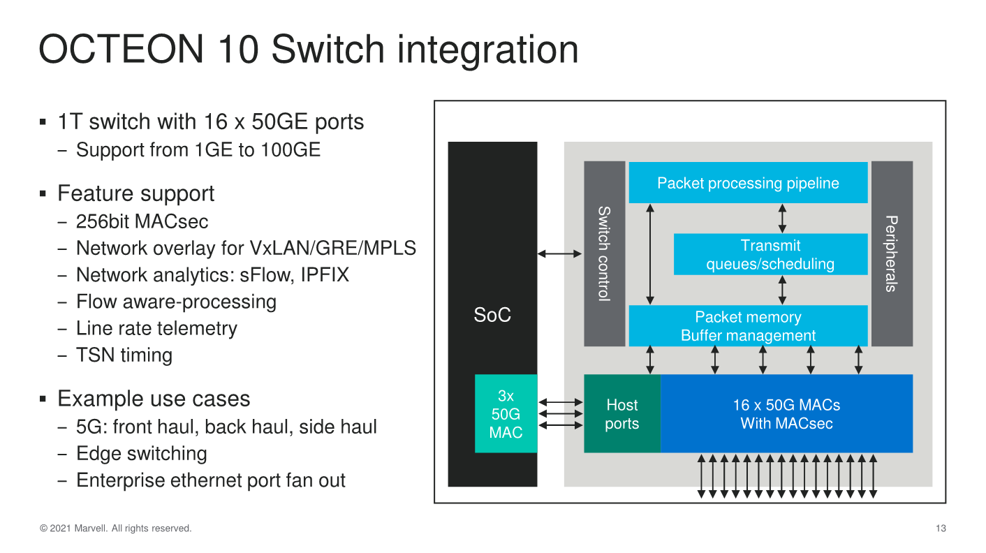
In terms of switch integration and network throughput, Marvell integrated a 1 Tb/s switch with up to 16 x 50G MACs – it’s not be noted though that the capabilities here are going to vary a lot based on the actual SKU and chip design in the family.
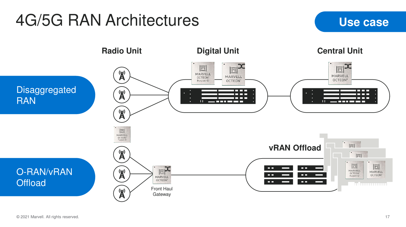
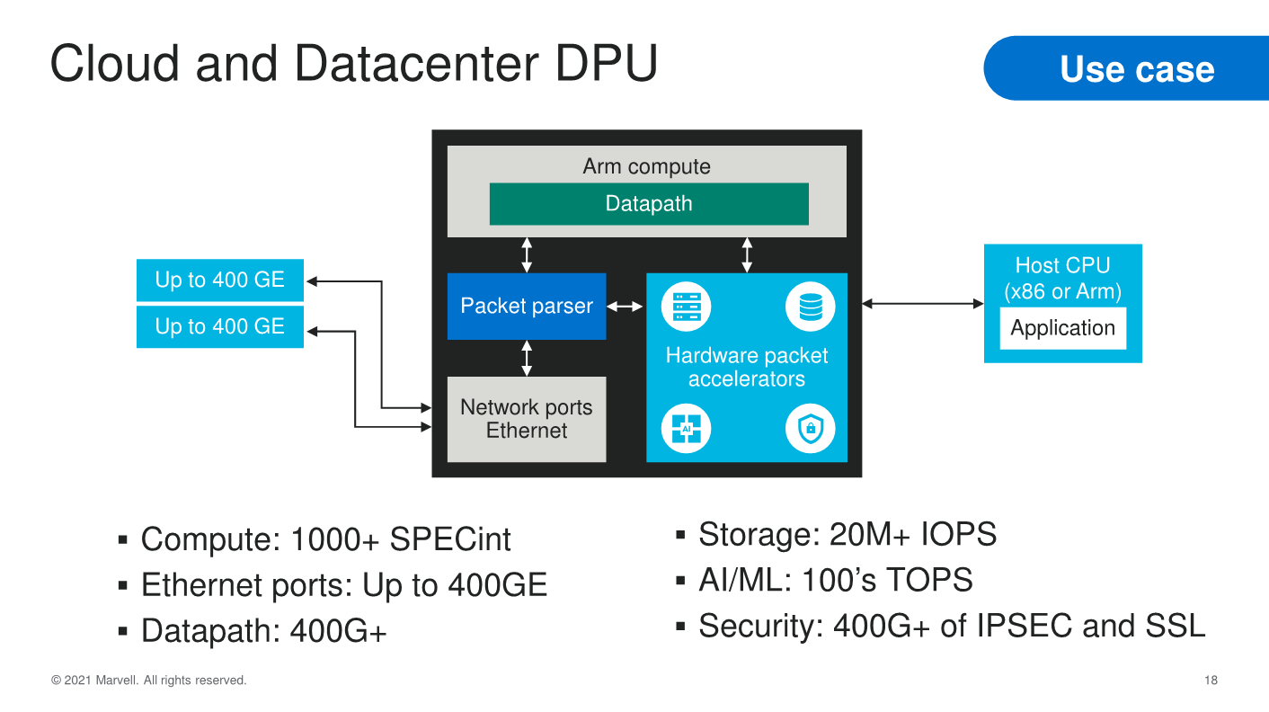
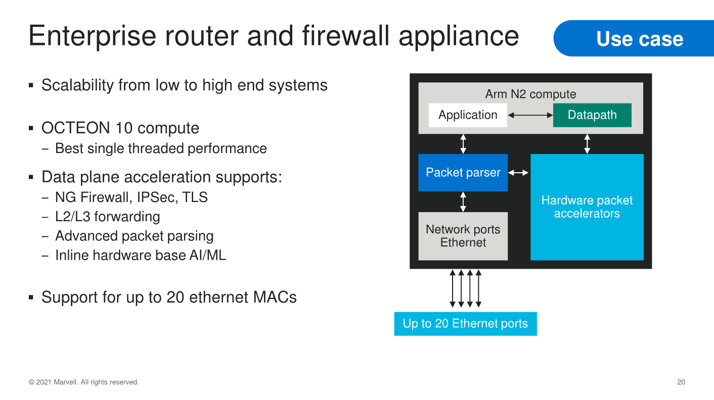
In terms of use-cases, the OCTEON 10 family covers a wide range of applications from the 4G/5G RAN Digital Units or Central Units, Front Haul Gateways or even vRAN Offload processors. In the cloud and datacentre, the solutions can offer a wide array of versatility in terms of compute and network throughput performance, while for enterprise use-cases, the family offers deeply integrated packet processing and security acceleration features.
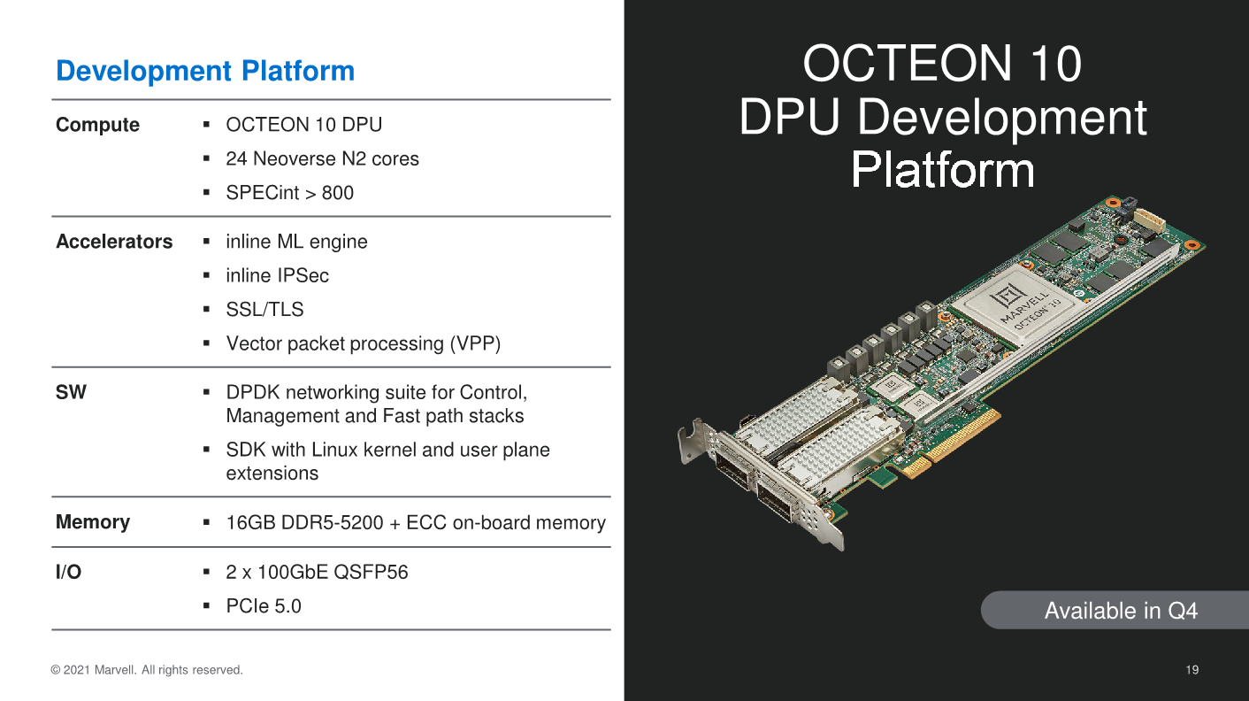
The first OCTEON 10 product and samples will be based on the CN106XX design with 24 N2 cores and 2x 100GbE QSFP56 ports on a PCIe 5.0 form-factor, available for Q4.
In terms of specifications, Marvell gives a breakdown of the various OCTEON 10 family designs:

Slide note: DDR5 controllers in this context refers to 40-bit channels (32+8bit ECC). Marvell also states that it still uses SPECint2006 due to its historical importance in regards to comparing to previous generation, and competitor solutions – it will publish 2017 estimates once the first silicon is ready.
The CN106XX is the first chip design of the OCTEON 10 family, taped out and expected to sample in the latter half of this year. Beyond this first chip, Marvell has 3 other OCTEON 10 designs in the form of the lower-end CN103XX with just 8 N2 cores and low TDPs of 10-25W, and two higher-end CN106XXS with improved network connectivity, and finally the DPU400 flagship with up to a massive 36 N2 cores and featuring the maximum amount of processing power and network connectivity throughput. What’s very exciting to see is that even with the largest implementations, the TDP only reaches 60W, which is far below the current generation CN98XX Octeon TX2 flagship implementation which lands in at 80-120W. These additional parts are yet to be taped out, and are planned to be sampled throughout 2022.
Marvell states that it’s been the industry leader in terms of DPU shipments, and is prevalent in all large datacentre deployments. This new Octeon 10 generation certainly seems extremely aggressive from a technology standpoint, featuring leading edge IP as well as manufacturing processes, which should give Marvell a notable advantage in terms of performance and power efficiency over the competition in the fast-evolving DPU market.


18 Comments
View All Comments
mode_13h - Friday, July 2, 2021 - link
I'm not entirely sold on the concept of vector packet processing. I wonder if they really wouldn't just be better off with >= 4-way SMT.brucethemoose - Friday, July 2, 2021 - link
Would security be a concern with SMT?For whatever reason, SMT seems to be unpopular in the ARM ecosystem, as even Marvell themselves abandoned the SMT heavy ThunderX3.
In fact, wasn't the TX2 processor based on ThunderX2, which was also a SMT4 design?
mode_13h - Saturday, July 3, 2021 - link
> Would security be a concern with SMT?I was just thinking about this. For some applications, no. This would tend to be running a highly-managed software stack. However, the nice thing about such an architecture is that you could run guest VMs and other sorts of software with higher likelihood of being malicious or exploitable to behave maliciously.
To help manage these risks, Linux now offers better policy control over which threads can share cores. So, you could limit core-sharing to threads of the same process or VM, for instance.
> For whatever reason, SMT seems to be unpopular in the ARM ecosystem,
Because ARM cores are traditionally comparatively small, the area-efficiency of SMT has been less.
ARM, itself, makes two SMT-2 cores (A65AE & A76AE), for 64-bit embedded applications. This is an implicit acknowledgement of the technical advantages of SMT. Embedded use-cases tend to be the ones with the least risk from side-channel attacks.
> as even Marvell themselves abandoned the SMT heavy ThunderX3.
I think that was simply because they weren't competitive with ARM's N2 cores.
mode_13h - Saturday, July 3, 2021 - link
> ... the area-efficiency of SMT has been less.I meant the benefit in area-efficiency vs. simply adding more cores.
Also, I think the raft of recent side-channel vulnerabilities has given SMT an image problem and reduced customer demand for the feature.
ChrisGX - Sunday, July 4, 2021 - link
I don't think Split-Lock capability in the Cortex-A76AE relies on SMT. Dual Core Lock-Step as the name suggests is a way of engaging two cores to raise the reliability of operations running on these specialised computing and control units.mode_13h - Sunday, July 4, 2021 - link
The split-lock functionality seems distinct from the SMT capability.https://www.anandtech.com/show/13727/arm-announces...
I'm not certain the A76AE is SMT-capable, however. That might've been some bad info I found.
ChrisGX - Monday, July 5, 2021 - link
Actually, I recall there was a second core besides the Cortex-A65AE from ARM with SMT - the Neoverse E1. Andrei pointed out that the E1 was derived from the Cortex-A65AE. At the time of the release of the E1 core ARM had thought it would be used for “throughput workloads that largely are...about shifting large amounts of data around" and that "are predominantly in the data plane". The Cortex-A65AE was said to be suited to streaming data from sensors whereas the E1 could support the streaming of data from the network in the case of infrastructure workloads. Evidently, with compute capability having become essential to DPUs - that is shown clearly by the Octeon 10 - the E1 may have been eclipsed in the role it was expected to play by ARM's N series Neoverse silicon.The SMT-capable A65 core still seems interesting to me. It wouldn't shock me to see it (or something very much like it) put to good use beyond Automotive applications in more mainstream Cortex parts.
https://www.anandtech.com/show/13959/arm-announces...
mode_13h - Wednesday, July 7, 2021 - link
Cool, I had forgotten about the E1. Thanks for the follow-up.This page includes a roadmap slide showing the E1, N2, and V1 all falling off a cliff labeled "Poseidon Generation", in 2022+. So, who knows if there'll be an E2 or whether it'll have any relation to the E1...
https://www.anandtech.com/show/16640/arm-announces...