EUV Pellicles Ready For Fabs, Expected to Boost Chip Yields and Sizes
by Anton Shilov on March 31, 2021 6:00 PM EST- Posted in
- Semiconductors
- EUV
- EUVL
- ASML
- TSMC
- Samsung Foundry
Foundries started limited usage of extreme ultraviolet (EUV) lithography for high-volume manufacturing (HVM) of chips in 2019. At the time, ASML's Twinscan NXE scanners were good enough for production, but the full EUV ecosystem was not quite there. One of the things that impacted EUV was the lack of protective pellicles for photomasks, which limited usage of EUV tools and affected yields. Fortunately, the situation with pellicles has finally improved thanks to the recent introduction of production-ready EUV pellicles, and matters promise to get even better in the coming years.
Protecting Precious Reticles
ASML has made a great progress with its Twinscan NXE EUV lithography tools in the recent years, improving performance of light source, availability time, and productivity. Its industry peers have also done a lot to make high-volume manufacturing (HVM) using EUV equipment possible. Still, the EUV ecosystem needs to develop further. One of the most notorious challenges the semiconductor supply chain faced with EUV is development of pellicles that were not available two years ago, which is why TSMC and Samsung Foundry had to invent ways how to use their EUV scanners without protective films.
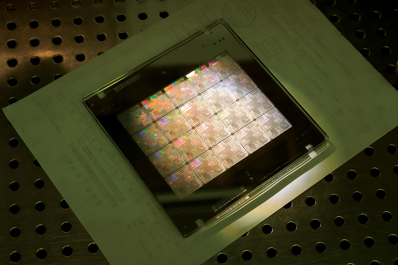
For Reference: A 16nm TSMC Pellicle With Reticle
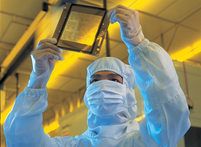
Pellicles protect 6×6-inch photomasks (reticles) during the chip production flow by sealing them away from particles that could land on their surface, which would otherwise damage them or introduce defects to wafers in production. Each reticle for an EUV tool costs $300,000, so chipmakers are eager to protect them against damage by particles or even the EUV radiation itself as this lowers their costs. Meanwhile, reducing risks associated with yields is perhaps even more important.
The need for pellicles, in turn, varies depending on the manufacturer and the types of photomasks employed. Intel, which is known for its big CPU dies, tends to use single-die reticles, which means that just one mask defect introduced by a particle automatically kills the whole die. Meanwhile, if a 25-die photomask is used, a particle adder will 'only' result in 4% lower yield (one dead die), which is why it's been possible to get away without pellicles for smaller chips and multi-die photomasks.
ASML Leading the Pack. For Now
The industry started to develop protective films for EUV tools relatively late after it transpired that nobody can guarantee that an ultra-complex EUV scanner is 100% free of harmful particles, which is why they were not ready in 2019.
Pellicles for photomasks to be used with deep ultraviolet (DUV) lithography equipment are common and cheap. By contrast, since photomasks for EUV are different from photomasks for DUV (EUV masks are essentially 250 to 350-nm thick stacks featuring 40 to 50 alternating layers of silicon and molybdenum on a substrate), pellicles for such reticles are also quite different. In particular, the very short wavelength of EUV means that pellicles for it have a number of requirements that make them uneasy to produce and expensive. EUV pellicles have to be extremely thin, should not affect reflection characteristics of reticles, should feature a high transmission rate (the higher the rate, the higher is productivity of a scanner), should sustain high EUV power levels, and withstand extreme temperatures (from 600ºC to 1,000ºC in the future).
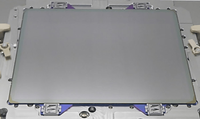
ASML's EUV Pellicle (Image Credit: Semiconductor Engineering)
"Most materials absorb very strongly at the more energetic 13.5nm EUV wavelength and, even when the most EUV-transparent materials are selected, the membranes must be extremely thin to approach 90% transmittance," said Emily Gallagher, a principal member of technical staff at Imec. "Such thin membranes are not usually capable of maintaining sufficient strength to be free-standing at the required dimensions. Additionally, the EUV scanner environment is not compatible with many materials and will subject the pellicle to pump-vent cycles."
To date, a number of EUV pellicle options have emerged, according to SemiEngineering:
- ASML introduced its first EUV pellicles in 2019 and licensed the technology to Mitsui Chemicals, which intends to start their volume sales in Q2 2021. Since then, ASML has improved its pellicles.
- Imec has disclosed test results of its pellicles based on carbon nanotubes.
- Graphene Square, Freudenberg Sealing Technologies (FST), and some universities are developing their own pellicles.
So far, only ASML has managed to create commercially viable pellicles for EUV tools that are actually available. ASML's pellicles are based on polysilicon that is 50 nm thick. Back in 2016, they demonstrated a 78% transmissions rate on a simulated 175W source. Currently ASML can sell a pellicle with an 88% transmission rate. And shortly, Mitsui will start supplying such pellicles in volume.
ASML's latest prototypes made of metal silicide demonstrate a 90.6% transmission rate with 0.2% non-uniformities and less than 0.005% reflectivity on a 400W source.
"This upgrade supports our roadmap, which eventually will take source power up to 400 Watts," said Raymond Maas, ASML’s product manager for pellicles, in an interview with Bits&Chips.nl. "The pellicle heats up to 600ºC at that power level, which the polysilicon couldn’t withstand."
By contrast, Imec's prototype pellicles have a transmission rate of 97.7%. In fact, in the long term, when more advanced light sources are available, more sophisticated pellicles will be needed and this is where Imec's carbon nanotubes-based pellicles will come into play.
"Few materials have the potential of high EUV transmission beyond 90% and even fewer materials are at the same time compatible with EUV powers beyond 600W. In addition, the pellicle needs to be strong to be suspended over a large area of the mask (~110mm x 140mm)," said Joost Bekaert, a researcher from Imec.
Unfortunately, it is unclear when Imec's carbon nanotube-based pellicles will be ready for primetime.
Summary
TSMC and Samsung Foundry have invented ways to use EUV lithography tools without pellicles on multi-die photomasks for smaller chips, but such methods are risky as any particle adder can become a yield killing defect. Furthermore, such methods are risky for bigger chips and single-die photomasks, so pellicles are critical for enabling large dies to be made with EUV tools. That said, regardless of the photomask size, pellicles are needed to improve EUV yields and reduce risks across the board.
Overall then, the use of and improvements in EUV pellicles will be a gradual process. The initial pellicles developed and made by ASML and soon to be made by Mitsui are good enough for some of today's needs, but there is room for improvement with their transmission levels, as evidenced by the next-generation prototypes developed by ASML and Imec. Better pellicles will be needed to account for future scanners as well, since those machines will have more powerful sources. Nonetheless, since such pellicles have a number of indisputable advantages, they are going to be used by chipmakers as they can help to improve yields even at the cost of some productivity.


34 Comments
View All Comments
Santoval - Thursday, April 1, 2021 - link
"In addition, the pellicle needs to be strong to be suspended over a large area of the mask.."How strong can a 50 nm thick membrane possibly be? The thinnest rice paper that can be made is about a micron (or μm) thick. That is 1/1000th of a mm or 1 millionth of a meter. These papers are so thin they are semi-transparent. These pellicles are 20 times thinner; so if you stack 20 of them on top of each other (assuming no air gaps at all) you get the same thickness as that super thin rice paper.
On top of needing to be strong despite being so thin they also need to be so rigid and thermally stable to withstand temperatures of 600 ºC or more and then back to room temperatures without breaking or deforming. I wonder how many such cycles they can endure and how expendable they are. If the precious EUV photomasks cost $300,000 a pop do their pellicles cost a couple of thousand bucks each or more (or less)?
edzieba - Thursday, April 1, 2021 - link
Commercial gold leaf is around 100nm, so 50nm ultra-thin films are not unreasonable. Paper is a terrible analogue as it is a fibrous composite, not a bulk material .Santoval - Thursday, April 1, 2021 - link
Paper is indeed a terrible analogue; while gold leaf can get so thin it is super fragile at such thickness, so I am not sure if it is a much better analogue. It also does not behave well with wide temperature changes due to a relatively high thermal expansion coefficient (~6 times higher than silicon).shabby - Thursday, April 1, 2021 - link
Intel: hello asml... we'd like to order some pellicles to boost our 10nm chip yieldsAsml: oh I get it, April fools 🤣
WaltC - Thursday, April 1, 2021 - link
I wonder if this sort of thing is behind the delay of AMD and nVidia GPUs ramping up for volume production. This shortage surely isn't because the globe has gone nuts over $600-$1500 GPUs...;) Those markets are small to begin with. My feeling is that the shortage is caused by poor yields at both FABs--it's as if they are waiting on something to happen before they begin to fill even the limited demand for these GPUs. I just wish AMD, especially, would come clean about the product shortage and stop with the "miner & unprecedented demand" cover ups. The demand cannot be "unprecedented" for a variety of reasons. 1) GPUs have never before cost this much, even @ their MSRPs--so there's no previous demand pattern to evaluate beyond "small" or even "tiny." 2) There has been no evidence in the last several months that either AMD or nVidia has been able to satisfy an "unprecedented demand" in any way, shape, or form. Everywhere you care to look for months all the sources are bare--bone dry--no AIB cards are being sold using either company's GPUs--nothing at the AMD store and nVidia has apparently stopped making its FE editions! There are none on Best Buy at all. It would be nice to hear a little honesty from both companies--the little trickle of these GPUs that has been produced and sold is far less than even normal new-GPU launches expect. Got to be serious yield problems slowing everything to a dead crawl.ballsystemlord - Thursday, April 1, 2021 - link
According to the youtube'r, moores law is dead, AMD has shipped over 500,000 5000 series CPUs.That sounds like an impressive demand to me. Esp. in Q1. Normally, according to the charts we see for company profits, it's a rather quiet first few months.
Spunjji - Friday, April 2, 2021 - link
"I just wish AMD, especially, would come clean about the product shortage and stop with the "miner & unprecedented demand" cover ups."You're asking them to lie to flatter your inaccurate take on the situation. Not gonna happen.
Tomatotech - Thursday, April 1, 2021 - link
Now this is proper *science*. I love this kind of reporting.It's a crying shame we don't get material like this coming out of Intel. They can fuck right off with their 'How wonderful gets done' PR materials.
TristanSDX - Friday, April 2, 2021 - link
The hidden secret is that EUV or even multiple patterning is not needed for increase density of chips. Main reason for disturbing (by diffraction rings) images are combination vawelength of light and density of features on mask. Increasing density of chips require decreasing vawelength of light, or increasing size of masks. First method (EUV) proved to be very difficult, while handling operate larger mask also have its disadvantages (reduced throughput) but overall is much easier. This is reason is why EUV was chosen, serious profits can be made by solving tougher problems. Making chips is business overall, and everyone involved want his money.jospoortvliet - Friday, April 2, 2021 - link
Wait, are you claiming making denser chips would have been possible in a more efficient, cheaper way than wit euv but to make one company rich (ASML) everybody in the industry including struggling intel and the Chinese companies desperate to get into cutting edge cpu designs all decided to ignore this cheap possibility and instead spent hundreds of billions on EUV? Sure, sounds totally legit, that is absolutely how capitalism works - leaving opportunities for massive profit on the floor to help another company.🦁