Intel Alder Lake: Confirmed x86 Hybrid with Golden Cove and Gracemont for 2021
by Dr. Ian Cutress on August 14, 2020 1:05 PM EST- Posted in
- CPUs
- Intel
- Alder Lake
- Hybrid
- Intel Arch Day 2020

Following leaks is often a game of cat and mouse – what is actually legitimate and what might not be. Traditionally AnandTech shies away from leaks for that very reason, and we prefer to have multiple sources that are saying the same thing, rather than addressing every potential rumor on the blogosphere. Nonetheless, hints towards a new product from Intel, Alder Lake, have been cropping up over the past few months, including getting a small mention in Intel’s Q2 2020 earnings. The leaks have suggested that it would offer a mixed Hybrid x86 environment similar to Intel’s current Lakefield product that uses high-performance cores paired with high-efficiency cores. As part of Intel’s Architecture Day 2020, the company officially announced Alder Lake as a hybrid x86 product on its roadmaps.
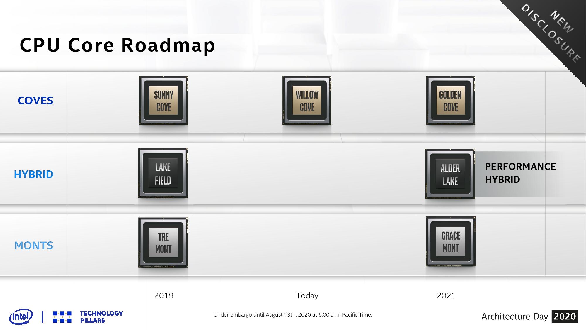
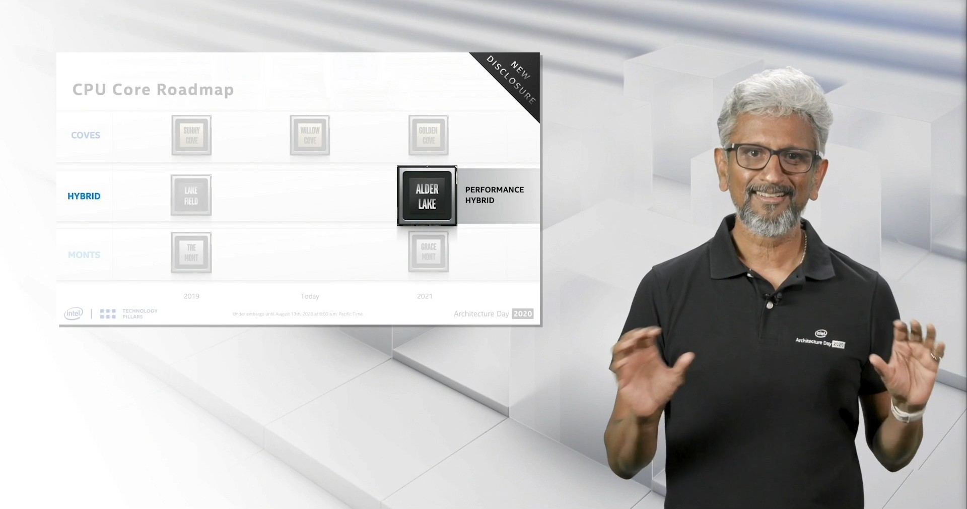
In the roadmap and as part of the discussions, Intel’s Raja Koduri confirms that Alder Lake will be a combination of the Golden Cove high performance computing core and the Gracemont high efficiency core, and the goal of this chip is to offer a ‘Performance Hybrid’ option into the portfolio. Raja explained to the audience that the company has learned a lot due to building Lakefield, its current hybrid x86 chip for thin and light notebooks, and while Lakefield was focused on battery life, Alder Lake will focus instead on performance.
Alder Lake will involve Intel’s next generation hardware scheduler, which we are told will be able to leverage all cores for performance and make it seamless to any software package. Intel claims that Alder Lake will be Intel’s best (ever? 2021?) performance-per-watt processor.
If leaks are to be believed, then Alder Lake looks set to offer an 8+8 design, although that has not been confirmed. Intel did not go into detail if Alder Lake will involve any next generation packaging, such as Foveros (which Lakefield does) – but in the Q2 2020 financial disclosures, it was said to be positioned for mobile and desktops. We expect Intel to discuss Golden Cove and Gracemont at some point next year, and then Alder Lake as an extension to those – we have already seen Intel documents regarding new instructions for each of these cores. My prediction is to come back this time next year, where we should have more to talk about.
Related Reading
- Intel Updates ISA Manual: New Instructions for Alder Lake, also BF16 for Sapphire Rapids
- Intel Roadmap Update: Alder Lake In H2’21, Ice Lake-SP Late This Year
- Intel’s 11th Gen Core Tiger Lake SoC Detailed: SuperFin, Willow Cove and Xe-LP
- The Intel Xe-LP GPU Architecture Deep Dive: Building Up The Next Generation
- The Intel Lakefield Deep Dive: Everything To Know About the First x86 Hybrid CPU


89 Comments
View All Comments
yeeeeman - Saturday, August 15, 2020 - link
Lakefield is not very competitive just because it is made on a shitty process...Unfortunately it is not made on this new SuperFin 10nm process, so the power/performance characteristics are similar to the 1065G7 which is pretty bad TBH.I would expect that Lakefield made on 7nm TSMC would be much much more competitive, allowing the Sunny Cove core to boost to ~3Ghz and the little ones to a similar frequency.
JayNor - Sunday, August 16, 2020 - link
22FFL base chiplet process of Lakefield offers ultra low leakage, which was required by MSFT's application.Spunjji - Monday, August 17, 2020 - link
I quite like the sound of those 2+8 chips - they could make for a really nice low-power experience. If they really have gone all the way down to 2+0 at the low end then that will be a shame - I can't imagine they'd have any yield reasons to do that as the small cores are so tiny, so it would entirely be about segmentation.brucethemoose - Friday, August 14, 2020 - link
I wonder if they'll start using Gracemont in big socket Xeons. Cloud providers would *love* to stuff 4 cores in the place of one big one in many scenarios, even if each core is a little (30%?) slower.Ian Cutress - Friday, August 14, 2020 - link
One of the issues with Hybrid right now is that you have to limit the support instructions to the lowest common denominator. So in a server, if you start adding Atom cores, you'll lose all the AVX512 stuff, which is just a waste of silicon. You can't just add different cores for free, it's always a bit of give and take.You could, technically, allow a hypervisor to build VMs of only one core type. But then you're just putting two different class of VMs onto the same CPU. Beyond that you can run into troubles regarding shared cache for one type of core, or how the LLC works, etc.
brucethemoose - Friday, August 14, 2020 - link
Thats not a problem if every core is a Gracemont core.But in future hybrid scenarios, I wonder if Intel will homogenize the ISA across the big and little cores. So a little core could, for example, accept an AVX 512 instruction, but it would break it down into a series of smaller ops that it can handle.
nandnandnand - Friday, August 14, 2020 - link
They should just use chiplets totaling 64 to 256+ Atom cores. Like Xeon Phi but with no AVX-512.Quantumz0d - Friday, August 14, 2020 - link
Makes sense, and I presume it won't be there in the Xeon lineup. I think many are not able to understand how does translate to performance. I hope AMD doesn't do this hybrid drama and rekts them straight with their Zen designs.lmcd - Friday, August 14, 2020 - link
This is why AVX512 is a dead end in the first place. Intel's Xe GPUs should be accelerating those instructions with the on-die Xe GPU accelerating if there's no dGPU. Intel doesn't hardly sell CPUs without GPUs anyway. Then that takes advantage of Intel's pricing for GPU virtualization as well, and eventually the possibility for GPU slices to be assigned out of a shared pool between the iGPU and dGPU.brucethemoose - Friday, August 14, 2020 - link
SIMD instructions and offloading to a GPU are very different. One can be done right inside a stream of branchy CPU instructions, or nice high level CPU code. With the other you have to start up a whole kernel and manually shuffle the data to and from the GPU, or let some library do it for you.Executing GPU instructions directly on data in system RAM, with a minimal latency hit, would be pretty awesome.