Testing a Chinese x86 CPU: A Deep Dive into Zen-based Hygon Dhyana Processors
by Dr. Ian Cutress & Wendell Wilson on February 27, 2020 9:00 AM ESTOur Hygon Systems
8-core Dhyana and Dual 32-core Dhyana Plus
The full range of Hygon’s known releases boils down to two platforms: one containing a single 8-core Zen 1 die, similar to the desktop range of processors (or EPYC 3000), and a set of server processors built from four dies in a similar arrangement to Naples.
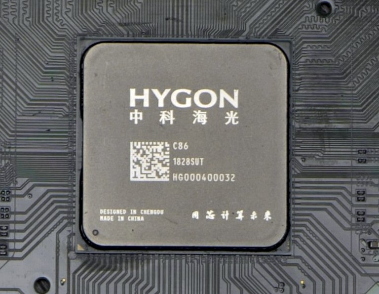
The 8-core engineering sample system we have in to test didn’t provide any exact SKU numbering – on the CPU it says ‘C86’ which is meant to imply ‘Chinese x86’. The rest of the numbering is likely linked to the wafer and batch that this silicon came from, however we do not have decoder rings for those.
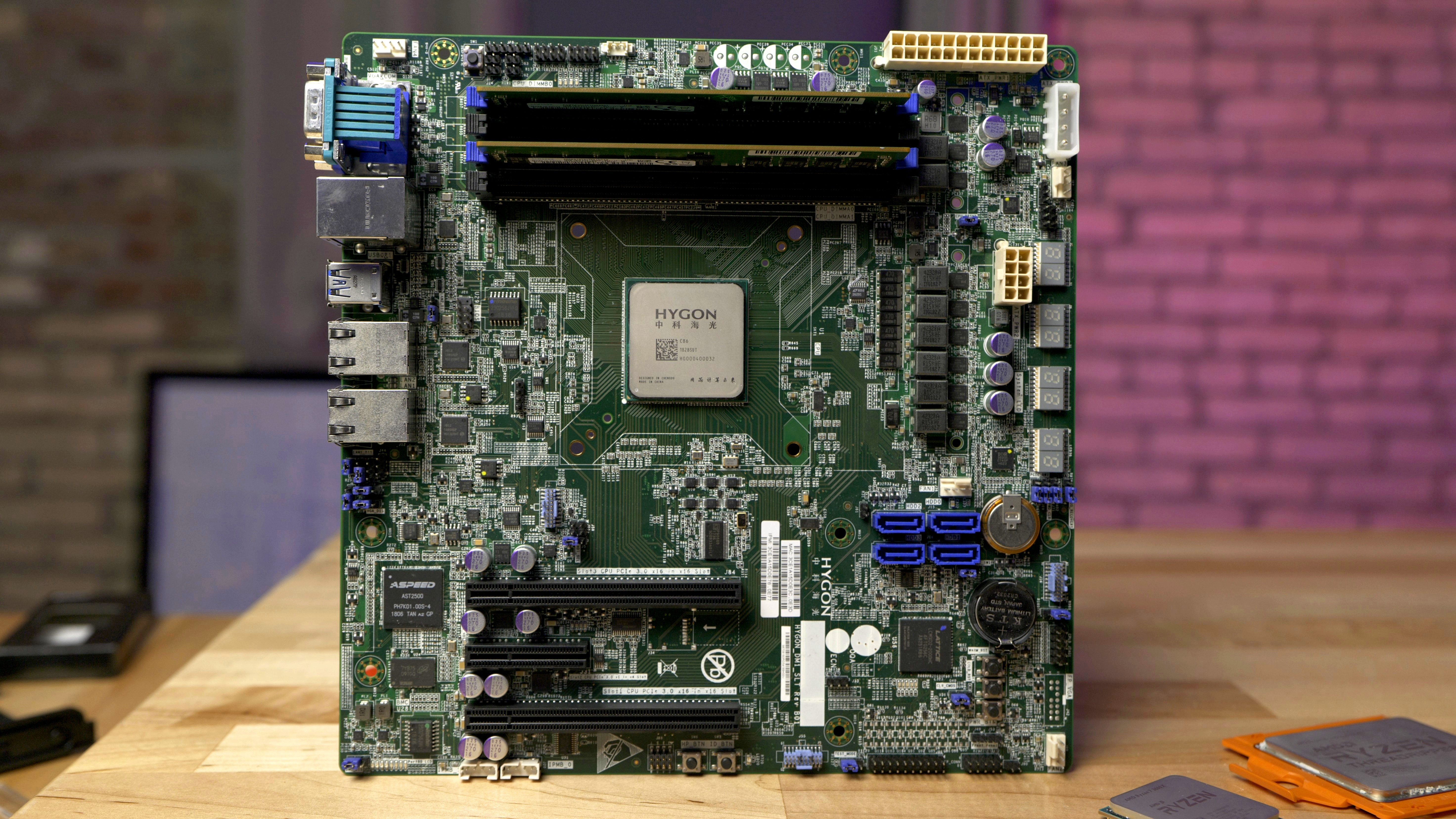
The motherboard uses a microATX form factor, and is very much a server motherboard with the DDR4 slots horizontal rather than vertical in order to direct airflow through the system in a server chassis. Starting primarily with the socket, what we have is a non-socketed BGA design, such that this CPU cannot be upgraded because it is bonded to the motherboard, similar to what we see with laptops and embedded systems. The mounting holes are the thing that surprises me here – these are not the AM4 mounting holes that we typically see with the consumer version of Ryzen, but these mounting holes are Intel mounting holes. Someone must have a lot of old Intel coolers around, I guess? Either that or it makes it easier for Hygon’s partners to find specific server grade coolers.
The CPU has a six-phase power delivery system, and as this is a pure CPU product, there is no integrated graphics. There is a form of 2D graphics provided by the IPMI controller in the bottom left, the classic ASPEED AST2500 chip that we commonly see in server systems. Unlike other microATX motherboards, there isn’t the typical four slot design here, but a three slot design, with two full length PCIe 3.0 slots (capable of x16/x0 or x8/x8) and an open ended PCIe x4 slot.
Normally these CPUs don’t really need a chipset because they have some SoC level IO functionality on the silicon, though consumer Ryzen CPUs were paired with X370 chipsets when the Ryzen 1000 family first launched. Instead of using those chipsets, Hygon has paired the CPU with a Lattice Semiconductor FPGA to act as a chipset of sorts. This gives the motherboard an odd set of combined IO, including SATA ports, four dual LED displays, a number of custom connectors and buttons, and a lot of undocumented things we don’t know. For example, there appears to be two batteries on the motherboard – one presumably to keep the onboard time, but the other seems more permanent and is not obvious why it is there.
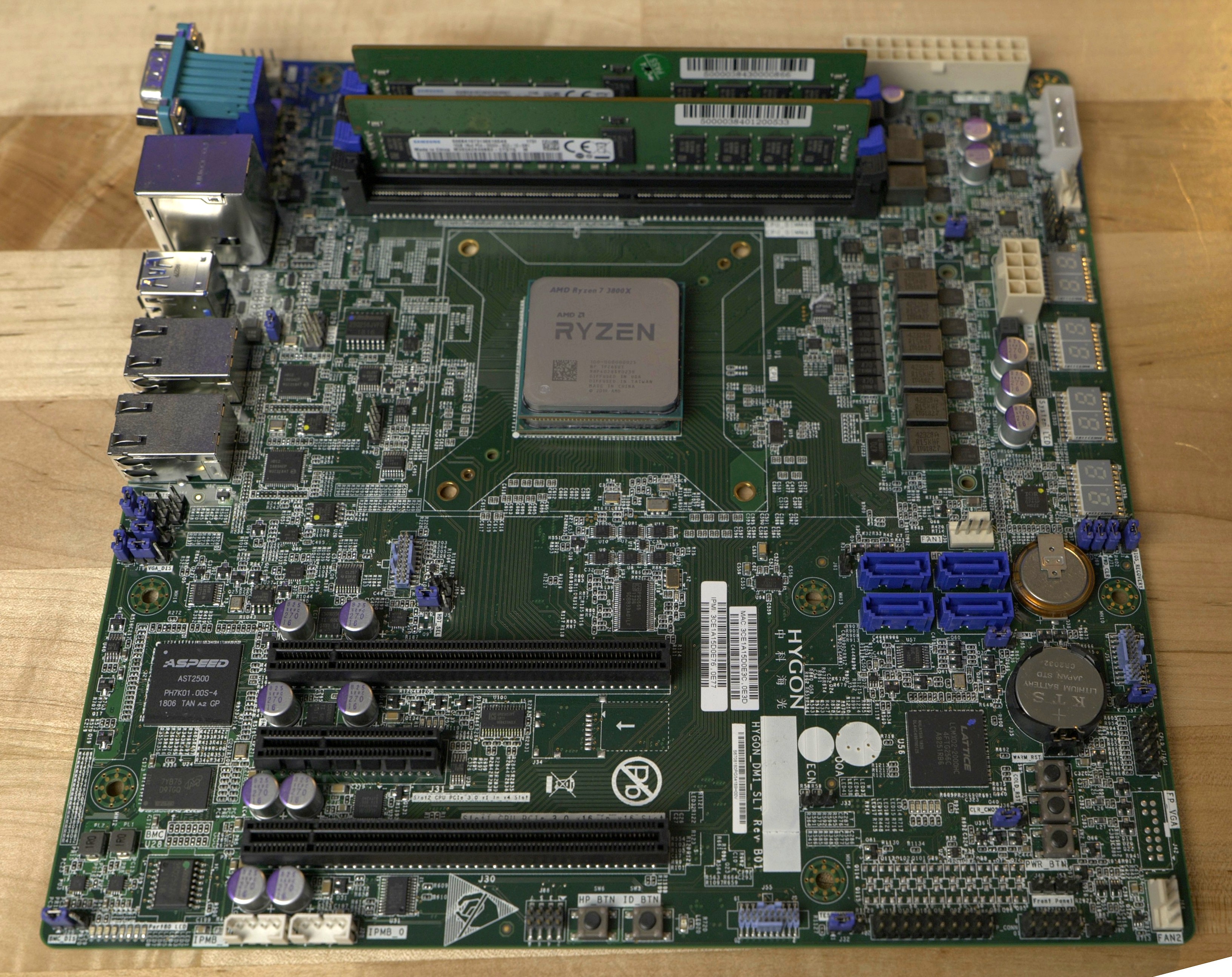
Here’s the motherboard where we’ve put an equivalent AM4 consumer Ryzen CPU on top, to show the size.

By comparison, the dual socket server is a bit of a beast. As we understand it, these servers were built for both compute and storage, with each CPU paired with four breakout connectors capable of four U.2 drives or 16-way SATA connectivity. The CPUs have eight channel memory capabilities, but due to a couple of reasons we had to test them in quad channel mode.
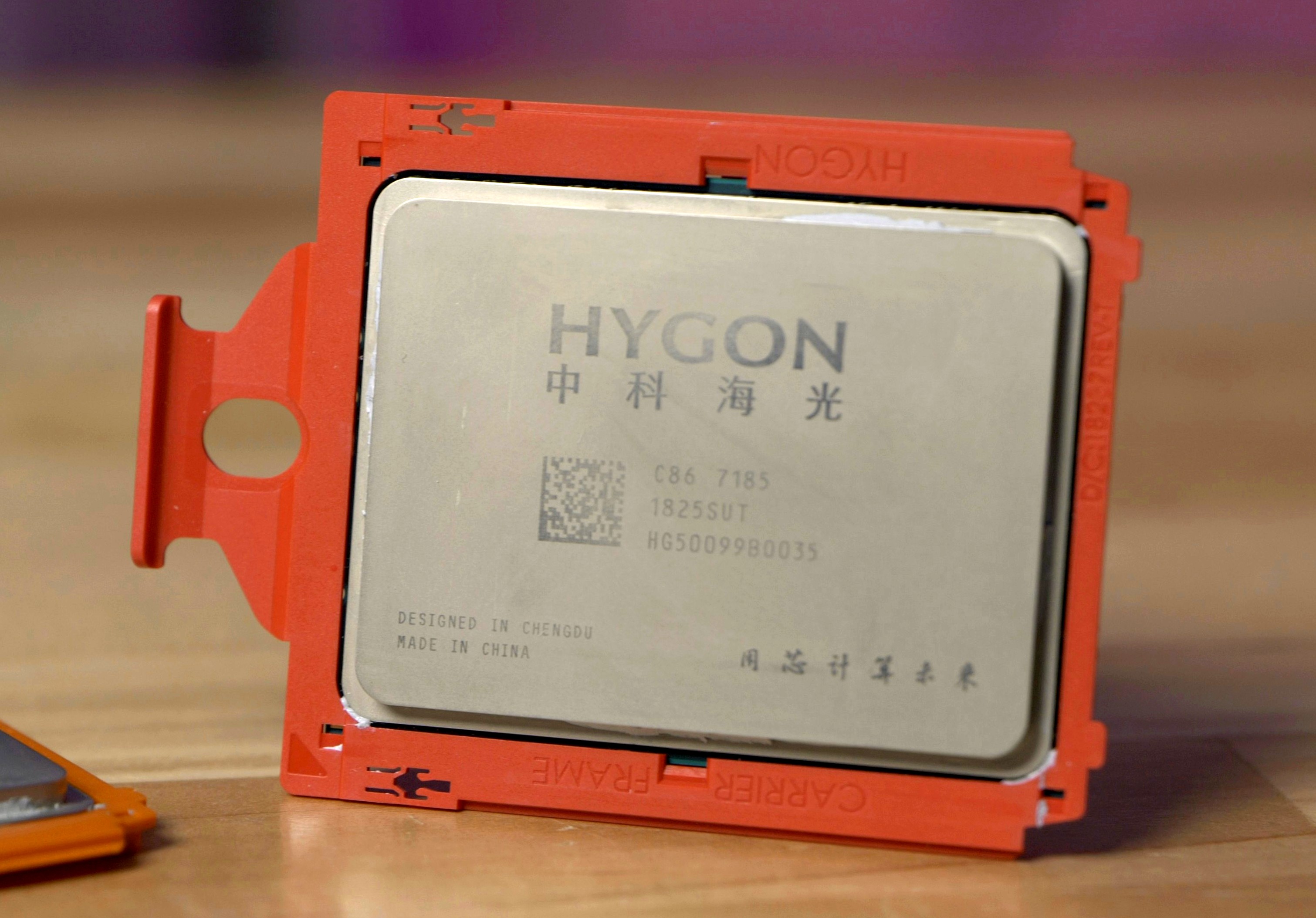
The CPUs in this case also say C86, but also have the model number 7185 on them, indicating a 32-core CPU. The carry case is red, whereas Naples EPYC CPUs were blue, Threadripper CPUs are orange, and Rome EPYC CPUs are green. The red might be a nod to the Chinese angle for these CPUs, however no-one we spoke to was able to confirm this.
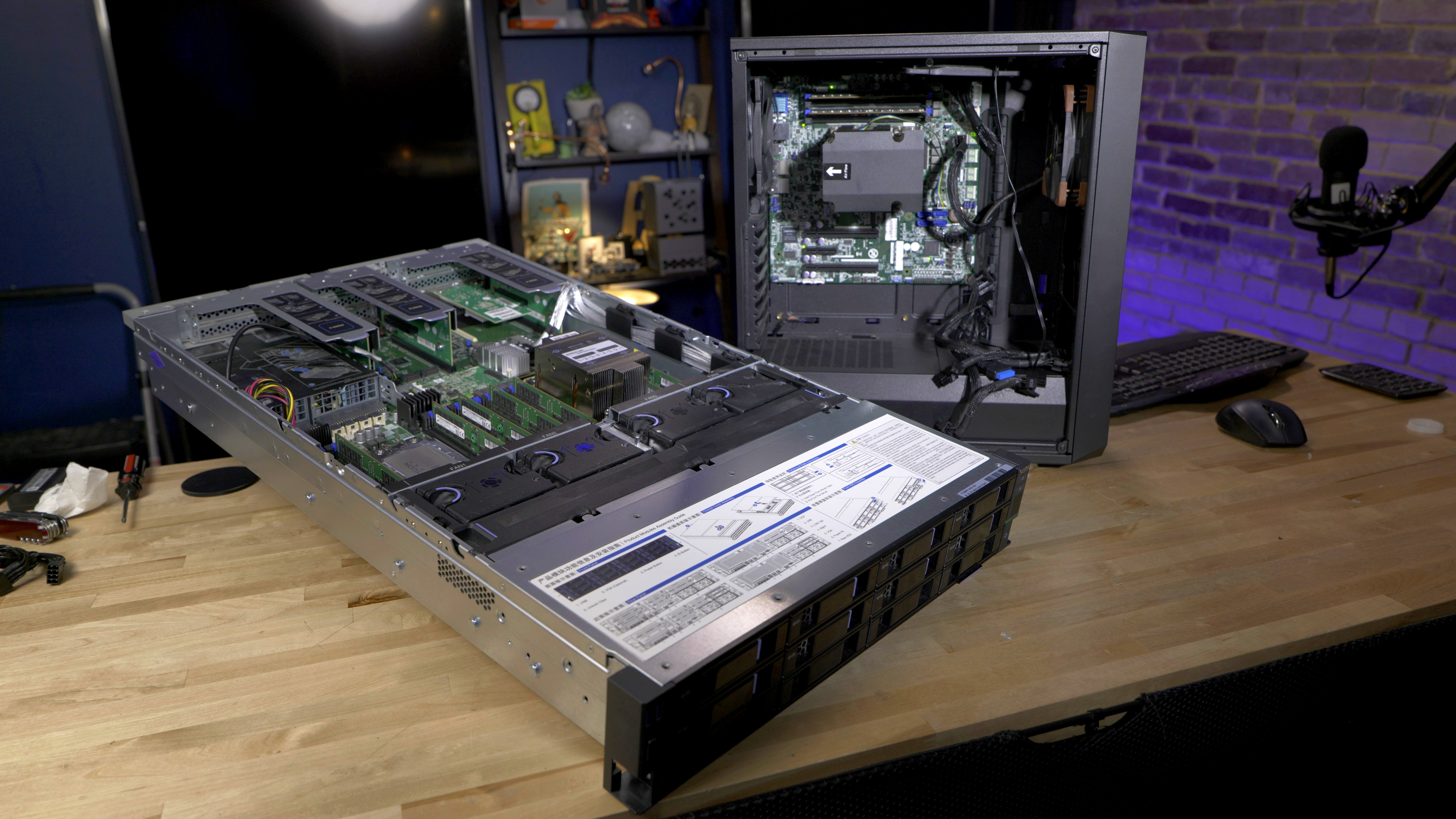
The server is actually a Sugon design, with 12 front panel 2.5-inch drive slots. For the 8-core system, that was put into a standard desktop case and fitted with a CPU cooler. Both systems were tested though remote desktop access, as Wendell was hosting them in his labs in Kentucky while I’m all the way back in London.
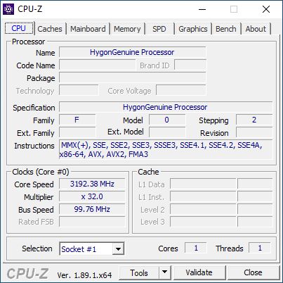
When trying to probe the CPUs, CPU-Z didn’t seem to have much of a clue. The software provided this interface on the 8-core consumer, showing a 3.2 GHz frequency, but only one core, and no other details aside from support for AVX, AVX2, and FMA3. For the server CPUs, CPU-Z failed to run at all. What we were able to determine is that the software thought that every core was a separate socket, and it appears that some of the usual ways to access this data on the AMD consumer CPUs have all been changed here for the Hygon models, either to evade detection using usual methods, or to conform to different standards. One interesting note is that while CPU-Z detected AVX and AVX2, some of our software couldn’t, and we had to revert to SSE detection in order to get that software to even run.


133 Comments
View All Comments
s.yu - Tuesday, March 3, 2020 - link
It says 2.40 ounces, that's the shipping weight but for something seemingly the size of a thumbnail I don't think it needs to be 2.4 ounces, not even with packaging.This 6 count battery bundle seems to have a shipping weight of 0.8 ounce.
https://www.amazon.com/Energizer-2032-BP-6-6-pack/...
Shadow7037932 - Sunday, March 8, 2020 - link
If you look at the datasheet, this CPLD doesn't need RAM backup. It's using Non volatile flash to store the config.Shadow7037932 - Sunday, March 8, 2020 - link
People in Asia/S.E. Area are using devices with HiSilicon Kirin SoCs, so I doubt they'll have issues exporting it.Soppro - Sunday, March 1, 2020 - link
This is very possible. China has done this in a variety of other areas such as high speed rail, mass transit and aircraft design/manufacturing, letting foreign companies to bid to gain access to the Chinese market and taking their proprietary technology in the process (foreign companies must partner with a Chinese counterpart). Case in point, Chinese HSR train sets have now improved to the point that they supersede the Japanese designs they were originally based on.khanikun - Monday, March 2, 2020 - link
That's how many countries do things. S.Korea's high speed trains originated from the French. Russia's high speed trains originated from the Germans. China's high speed trains originated from the Japanese, French, and Germans. You build upon what you learned and if they didn't want to make a new rival, they shouldn't have trained them on how to build high speed trains, just so they could try to gain a new market share.I say just sell at a high price, to make up for these future losses, if you want to sell to China or ignore the market. Course that could also just wind up with the Chinese trying to steal your tech via hacking or whatever else.
evernessince - Thursday, February 27, 2020 - link
Licensed, not sold.SSNSeawolf - Thursday, February 27, 2020 - link
This is the most excited I've ever gotten about someone violating import restrictions. There's a lot of strange stuff to parse through here.1.) I'd be interested to see where the second battery's traces lead; that should help solve the mystery.
2.) I'd like to see Linux booted up and have a look at lscpu. That will probably be more helpful than CPU-Z for these chips.
3.) The Intel cooler thing is just bizarre. The cooler IP must not have been licensed, which is also an interesting nugget.
4.) I'd be very interested in having someone take a hard look at the chipset FPGA.
5.) Tangential, but I wonder if the BMC has been modified in any way.
Kevin G - Thursday, February 27, 2020 - link
The Intel cooler is indeed odd but it isn't unique. There is an AM4 with Intel LGA115x mounts: the Asrock X570 Phantom Gaming-ITX/TB3 is one such board.I'll second the need to dig into the FGPA. If there is any major truth to what the tin-foil hatters are saying, that is the prime location to put a backdoor since that is reprogrammable. Outside of that, it does appear the consumer board has a SD card slot and a USB 3.0 header silk screened. I wonder if they were soldered on if they'd be active in any sort of capacity or if they're disabled out of necessity by not having enough resources on the FPGA.
I'll second that BMC differences would just be interesting.
Slash3 - Thursday, February 27, 2020 - link
I'm a bit surprised that the cooler mount even elicited as much as a raised eyebrow from Ian, as it's definitely been done before to utilize the smaller dimensions. Some things really are as obvious as they seem, and nothing more.myself248 - Wednesday, March 18, 2020 - link
Is that a microSD slot? I was thinking it might be a SIM slot. Either way, super interesting, and I would love to see that FPGA bitstream analyzed. There are folks who can make some sense of such things, I am not one of them.