Intel Joins CHIPS Alliance, Contributes Advanced Interface Bus
by Anton Shilov on January 24, 2020 11:00 AM EST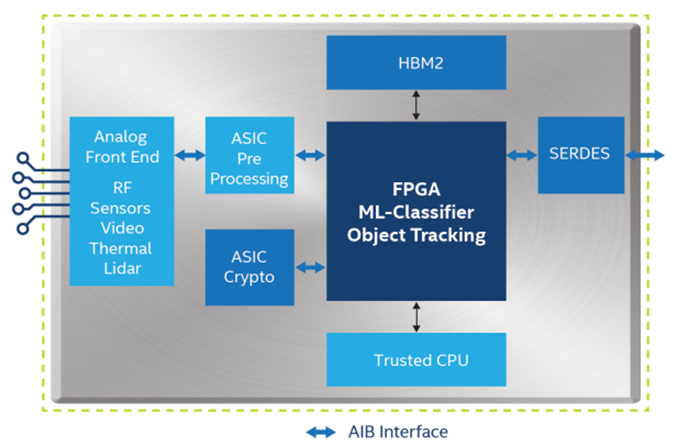
Intel this week became a member of CHIPS Alliance, an industry consortium that is working to accelerate the development of open source SoCs (and SiPs) for various applications. As part of their membership, Intel has also contributed its Advanced Interface Bus to the group, giving developers access to the bus and thus the means to interoperate with Intel (and other) chips that will be using it.
Designed for use with system-in-packages (SiPs) devices, Intel’s AIB is a high-bandwidth, low-power, die-to-die PHY level standard that uses a clock forwarded parallel data transfer mechanism (akin that used by modern DDR DRAM interfaces). The technology is agnostic to manufacturing processes and packaging technology, so it can be used to connect a wide variety of chips/chiplets using different types of packages, including Intel’s own EMIB, TSMC’s CoWoS, or other 2.5D technologies from numerous vendors.
Intel’s AIB has been available to third parties on a royalty-free basis for a while now, so contributing the technology to CHIPS Alliance is the next step for Intel in increasing its adoption. By making AIB available to a very broad group of chip designers, Intel is encouraging development of an ecosystem of chiplets that can later be used with its own CPUs, GPUs, FPGAs, and other components to build special-purpose multi-die SiPs.
Now that CHIPS Alliance controls Advanced Interface Bus specification, further development of the technology will be handled by its Interconnects workgroup, which is set to begin its operations shortly. As a part of the consortium, Intel will be able to further contribute to development of AIB. Meanwhile, Intel will get a seat on the governing board of CHIPS Alliance.
Dr. Zvonimir Bandić, Chairman, CHIPS Alliance, and senior director of next-generation platforms architecture at Western Digital said the following:
“Intel’s selection of CHIPS Alliance for the AIB specifications affirms the leading role that the organization impacts for open source hardware and software development tools. We look forward to faster adoption of AIB as an open source chiplet interface.”
Related Reading:
- Intel Provides Royalty-Free License for Data Bus to DARPA’s Modular Chips Initiative
- An Interconnected Interview with Intel’s Ramune Nagisetty: A Future with Foveros
- Intel’s Xe for HPC: Ponte Vecchio with Chiplets, EMIB, and Foveros on 7nm, Coming 2021
- Intel’s EMIB Now Between Two High TDP Die: The New Stratix 10 GX 10M FPGA
- Arm Joins CXL Consortium
- AMD Joins CXL Consortium: Playing in All The Interconnects
- Compute Express Link (CXL): From Nine Members to Thirty Three
- CXL Specification 1.0 Released: New Industry High-Speed Interconnect From Intel
- Gen-Z Interconnect Core Specification 1.0 Published
Source: CHIPS Alliance


17 Comments
View All Comments
name99 - Friday, January 24, 2020 - link
This is precisely the scenario I DON'T buy. If you want an NPU, stick it on the damn SoC. There is only downside, zero upside to having it as a separate chiplet.Chiplets mainly worls for separate physical substrate.
So
- RF (but that's already handled by separate chip, chiplet just gets you a little power/space savings),
- optical (people been talking about this for years, but if you can get Si photonics to work, again on SoC is better)
- MRAM (maybe maybe maybe? but we've all been burned by talking up the eminent arrival of MRAM in consumer products)
- cheaper IO hub ala AMD (this is the one realistic case --- but also the case that is least likely to require standardized connectivity...)
Kakti - Saturday, January 25, 2020 - link
The obvious usecase based on the diagram provided is for self-driving cars or perhaps industrial manufacturing equipment such as CNCs and robotic welding tools. This is an interconnect to link a variety of sensors to the processing CPU, with inputs coming from:1) Analog front end (operator touchscreen and physical buttons)
2) RF (radio frequency) reception/broadcast (cars or tolls talking to each other over low power maybe?)
3) Sensors (water, air pressure, sudden acceleration/deceleration, etc),
4) Video (back up cam amongst other uses)
5) Thermal (checking battery/capacitor/ICE temperatures)
6) Lidar (self-driving support, used by several Tesla competitors). Radar uses radio waves to bounce an electromagnetic signal off an object and counting the time it takes to return to calculate distance/speed, LIDAR uses optical lasers instead of radiowaves.
Fataliity - Friday, January 24, 2020 - link
I see this being used for Hyperscalers. Platinum members are Ali, Google, etc.They can put their TPU connected directly to Intel CPU on substrate. Same wiht Ali's new Samsung AI accelerator. And Intel's Habana Labs AI solution.
They're already making their own silicon. Why not keep yourself in the loop by being the CPU they decide to connect to? SiFive's in there. So if Intel doesn't do it, ARM/RISC will.
mode_13h - Saturday, January 25, 2020 - link
Those guys also make embedded solutions, even if you mostly think of them as playing in the cloud.alufan - Sunday, January 26, 2020 - link
clever move making sure Intels chips are not designed out of the landscape, this is the way AMD needs to start thinking because everything that Intel does (rightly) ensures they are always a consideration for future designs. As a potential shareholder it would impress me the amount of forward thinking they demonstrateNikTerry - Friday, February 28, 2020 - link
Hello there,Does anyone know where can i find some more deatild specs for the AIB blocks?(AFE or SerDes)
Thank you
Nik
dorcassmith - Monday, March 2, 2020 - link
In an era where Top Essay Writing are thriving, it has become increasingly difficult for students to identify with a reliable company that offers Best Essay Writing Services and Top Essay Writing Services.https://topessaywriting.com/