NVIDIA Details DRIVE AGX Orin: A Herculean Arm Automotive SoC For 2022
by Ryan Smith on December 18, 2019 8:30 AM EST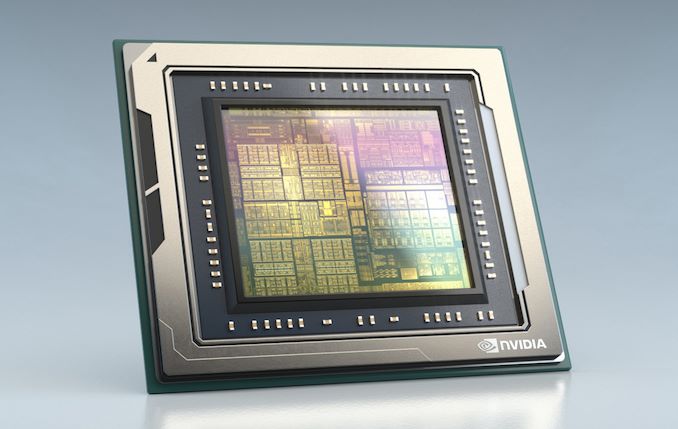
While NVIDIA’s SoC efforts haven’t gone entirely to plan since the company first started on them over a decade ago, NVIDIA has been able to find a niche that works in the automotive field. Backing the company’s powerful DRIVE hardware, these SoCs have become increasingly specialized as the DRIVE platform itself evolves to meet the needs of the slowly maturing market for the brains behind self-driving cars. And now, NVIDIA’s family of automotive SoCs is growing once again, with the formal unveiling of the Orin SoC.
First outlined as part of NVIDIA’s DRIVE roadmap at GTC 2018, NVIDIA CEO Jensen Huang took the stage at GTC China this morning to properly introduce the chip that will be powering the next generation of the DRIVE platform. Officially dubbed the NVIDIA DRIVE AGX Orin, the new chip will eventually succeed NVIDIA’s currently shipping Xavier SoC, which has been available for about the last year now. In fact, as has been the case with previous NVIDIA DRIVE unveils, NVIDIA is announcing the chip well in advance: the company isn't expecting the chip to be fully ready for automakers until 2022.
What lies beneath Orin then is a lot of hardware, with NVIDIA going into some high-level details on certain parts, but skimming over others. Overall, Orin is a 17 billion transistor chip, almost double the transistor count of Xavier and continuing the trend of very large, very powerful automotive SoCs. NVIDIA is not disclosing the manufacturing process being used at this time, but given their timeframe, some sort of 7nm or 5nm process (or derivative) is pretty much a given. And NVIDIA will definitely need a smaller manufacturing process – to put things in comparison, the company’s top-end Turing GPU, TU102, takes up 754mm2 for 18.6B transistors, so Orin will pack in almost as many transistors as one of NVIDIA’s best GPUs today.
| NVIDIA ARM SoC Specification Comparison | |||||
| Orin | Xavier | Parker | |||
| CPU Cores | 12x Arm "Hercules" | 8x NVIDIA Custom ARM "Carmel" | 2x NVIDIA Denver + 4x Arm Cortex-A57 |
||
| GPU Cores | "Next-Generation" NVIDIA iGPU | Xavier Volta iGPU (512 CUDA Cores) |
Parker Pascal iGPU (256 CUDA Cores) |
||
| INT8 DL TOPS | 200 TOPS | 30 TOPS | N/A | ||
| FP32 TFLOPS | ? | 1.3 TFLOPs | 0.7 TFLOPs | ||
| Manufacturing Process | 7nm? | TSMC 12nm FFN | TSMC 16nm FinFET | ||
| TDP | ~65-70W? | 30W | 15W | ||
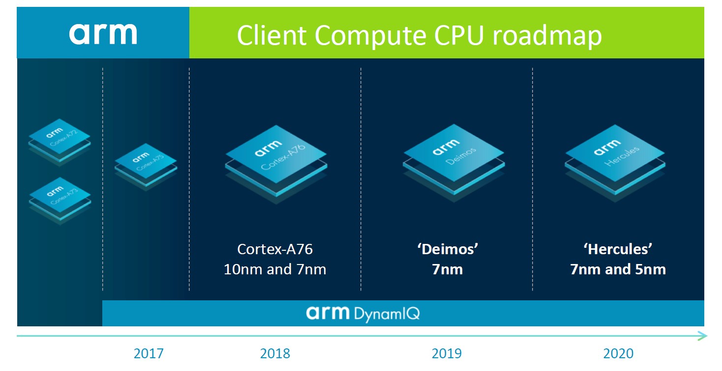
Those transistors, in turn, will be driving several elements. Surprisingly, for today’s announcement NVIDIA has confirmed what CPU core they’ll be using. And even more surprisingly, it isn’t theirs. After flirting with both Arm and NVIDIA-designed CPU cores for several years now, NVIDIA has seemingly settled down with Arm. Orin will include a dozen of Arm’s upcoming Hercules CPU cores, which are from Arm’s client device line of CPU cores. Hercules, in turn, succeeds today’s Cortex-A77 CPU cores, with customers recently receiving the first IP for the core. For the moment we have very little information on Hercules itself, but Arm has previously disclosed that it will be a further refinement of the A76/A77 cores.
I won’t spend too much time dwelling on NVIDIA’s decision to go with Arm’s Cortex-A cores after using their own CPU cores for their last couple of SoCs, but it’s consistent with the direction we’ve seen most of Arm’s other high-end customers take. Developing a fast, high-performance CPU core only gets harder and harder every generation. And with Arm taking a serious stab at the subject, there’s a lot of sense in backing Arm’s efforts by licensing their cores as opposed to investing even more money in further improving NVIDIA’s Project Denver-based designs. It does remove one area where NVIDIA could make a unique offering, but on the flip side it does mean they can focus more on their GPU and accelerator efforts.
Speaking of GPUs, Jensen revealed very little about the GPU technology that Orin will integrate. Besides confirming that it’s a “next generation” architecture that offers all of the CUDA core and tensor functionality that NVIDIA has become known for, nothing else was stated. This isn’t wholly surprising since NVIDIA hasn’t disclosed anything about their forthcoming GPU architectures – we haven’t seen a roadmap there in a while – but it means the GPU side is a bit of a blank slate. Given the large gap between now and Orin’s launch, it’s not even clear if the architecture will be NVIDIA’s next immediate GPU architecture or the one after that, however given how Xavier’s development went and the extensive validation required for automotive, NVIDIA’s 2020(ish) GPU architecture seems like a safe bet.
Meanwhile NVIDIA’s Deep Learning Accelerator (DLA) blocks will also be making a return. These blocks don’t get too much attention since they’re unique to NVIDIA’s DRIVE SoCs, but these are hardware blocks to further offload neural network inference, above and beyond what NVIDIA’s tensor cores already do. On the programmable/fixed-function scale they’re closer to the latter, with the task-specific hardware being a good fit for the power and energy-efficiency needs NVIDIA is shooting for.
All told, NVIDIA expects Orin to deliver 7x the 30 INT8 TOPS performance of Xavier, with the combination of the GPU and DLA pushing 200 TOPS. It goes without saying that NVIDIA is still heavily invested in neural networks as the solution to self-driving systems, so they are similarly heavily investing in hardware to execute those neural nets.
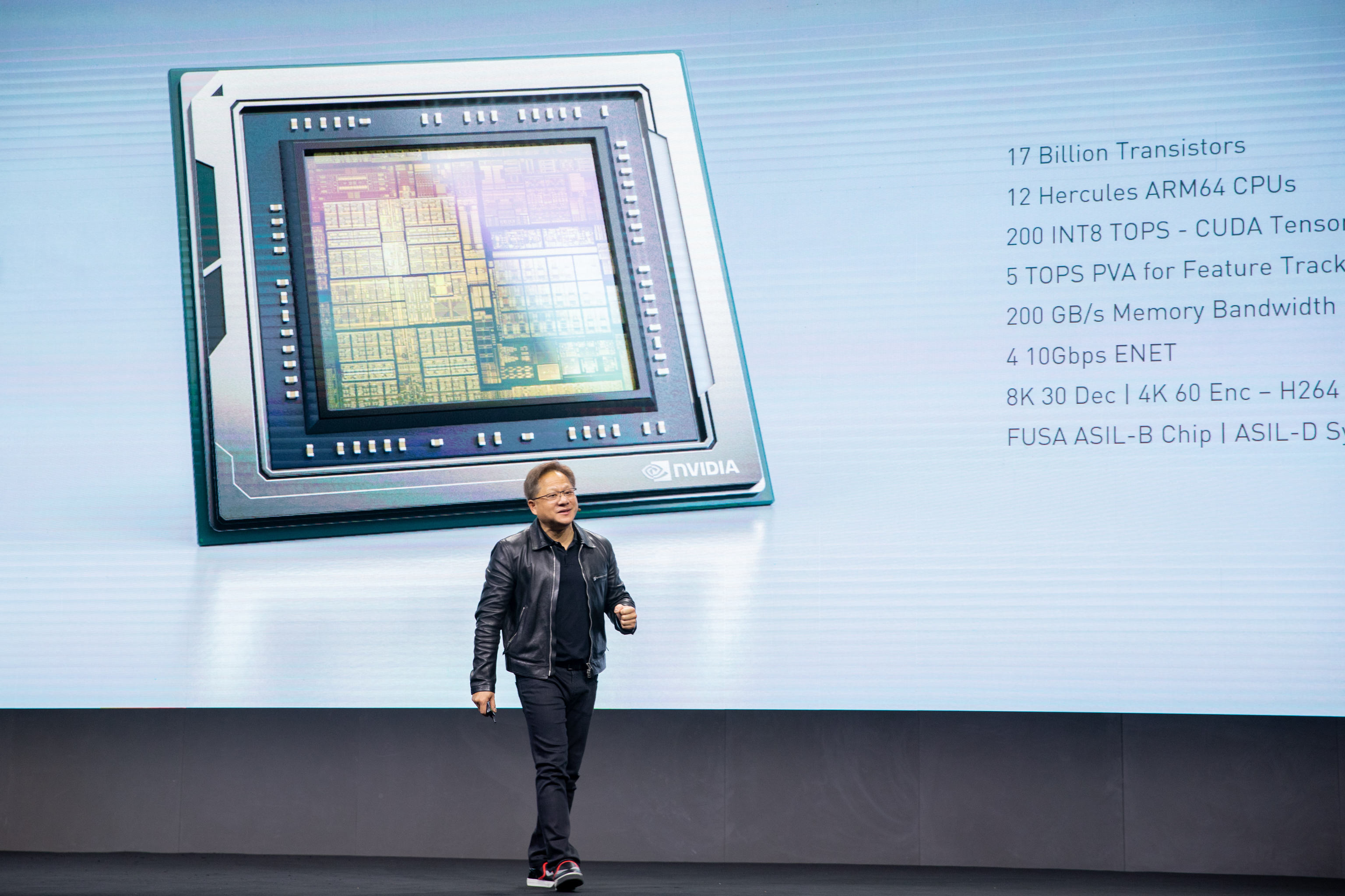
Rounding out the Orin package, NVIDIA’s announcement also confirms that the chip will offer plenty of hardware for supporting features. The chip will offer 4x 10 Gigabit Ethernet hosts for sensors and in-vehicle communication, and while the company hasn’t disclosed how many camera inputs the SoC can field, it will offer 4Kp60 video stream encoding and 8Kp30 decoding for H.264/HEVC/VP9. The company has also set a goal for 200GB/sec of memory bandwidth. Given the timeframe for Orin and what NVIDIA does for Xavier today, an 256-bit memory bus with LPDDR5 support sounds like a shoe-in, but of course this remains to be confirmed.
Finally, while NVIDIA hasn’t disclosed any official figures for power consumption, it’s clear that overall power usage is going up relative to Xavier. While Orin is expected to be 7x faster than Xavier, NVIDIA is only claiming it’s 3x as power efficient. Assuming NVIDIA is basing all of this on INT8 TOPS as they usually do, then the 1 TOPS/Watt Xavier would be replaced by the 3 TOPS/Watt Orin, putting the 200 TOPS chip at around 65-70 Watts. Which is admittedly still fairly low for a single chip at a company that sells 400 Watt GPUs, but it could add up if NVIDIA builds another multi-processor board like the DRIVE Pegasus.
Overall, NVIDIA certainly has some lofty expectations for Orin. Like Xavier before it, NVIDIA intends for various forms of Orin to power everything from level 2 autonomous cars right up to full self-driving level 5 systems. And, of course, it will do so while being able to provide the necessary ASIL-D level system integrity that will be expected for self-driving cars.
But as always, NVIDIA is far from the only silicon vendor with such lofty goals. The company will be competing with a number of other companies all providing their own silicon for self-driving cars – ranging from start-ups to the likes of Intel – and while Orin will be a big step forward in single-chip performance for the company, it’s still very much the early days for the market as a whole. So NVIDIA has their work cut out for them across hardware, software, and customer relations.
Source: NVIDIA


33 Comments
View All Comments
Yojimbo - Friday, December 20, 2019 - link
When the Switch was announced, NVIDIA talked about a long-term partnership with Nintendo. I think something like 20 years was mentioned. I'm pretty sure the Switch has high enough volumes to warrant NVIDIA creating an SoC for it. That SoC can also be used for Shield devices, wearables, and future generations of infotainment processors. I don't think NVIDIA is interested in doing the bare minimum to increase performance. They will either make the SoC, in which case it will be up to Nintendo how much they want to pay to get what level of performance, or they won't. They will have all the pieces in place to make as powerful an SoC as Nintendo might request.jeremyshaw - Thursday, December 19, 2019 - link
Nvidia has always chosen whichever CPU is more prudent at the moment - no vanity in forcing a CPU design into a product just to show off, like Samsung (or Qualcomm in the past). This isn't the first time they have "ditched" their in-house ARMv8 design "in favor" of ARM.TheinsanegamerN - Wednesday, December 18, 2019 - link
I miss the tegra chips. Shame Nvidia never bothered to support that line any further.drexnx - Wednesday, December 18, 2019 - link
something about them just didn't play nice with LTE modems, that's what really killed the Tegra lineYojimbo - Wednesday, December 18, 2019 - link
NVIDIA couldn't get past Qualcomm's stranglehold on the smartphone market due to Qualcomm's modem capabilities. NVIDIA accused Qualcomm of being anticompetitive and Qualcomm were eventually fined for just that, but by that time NVIDIA had exited the market. NVIDIA tried to target the tablet market but the non-ipad tablet market never really took off and they abandoned that too and pivoted to in-car infotainment systems. They found the margins there too low for their liking and so now are re-pivoting to autonomous machines (self driving cars and robots) and automotive AI cockpits, as well as the Nintendo Switch and the Shield TV, the last of which probably only still exists because of the Switch.Raqia - Wednesday, December 18, 2019 - link
The main issue was that their Icera unit employed soft modems that were never going to be competitive with hardware accelerated solutions from other vendors.Yojimbo - Wednesday, December 18, 2019 - link
Maybe. I never really saw any comparisons. There certainly was room at the time for vendors to try the soft modem or use two chips solutions. Qualcomm was found to have sold their modem chipsets below cost to force Icera out of the market, that is something I do know.Raqia - Wednesday, December 18, 2019 - link
That was the EU's interpretation of a pricing discount on a very low volume of chip shipments whereas the average cost over the lifetime of a contract was in no way below cost or anticompetitive. Cost recovery is a standard business practice and didn't affect the longer term business decisions here: the main issue remains that Icera didn't have a competitive modem with which to secure a longer term contract.Yojimbo - Friday, December 20, 2019 - link
Qualcomm's anti-competitive practices both affected the long term business decisions and the EU's decision. I'm not sure what you are trying to say here. If the EU felt that the reason Icera failed was because of an inferior product then there woul dbe no reason to issue the ruling.Karmena - Friday, December 20, 2019 - link
LTE was not integrated into them. That is the issue. Apple had/have the same issue - if you see battery tests for iPhones on wifi or on 4G there is a stark contrast. While everyone praises high-power cores the beast lives in low power cores for background tasks and this is where A55 (or whatever) fails.