Hot Chips 31 Live Blogs: Intel Lakefield and Foveros
by Dr. Ian Cutress on August 20, 2019 7:10 PM EST
07:14PM EDT - One of the interesting developments in packaging technology in recent memory is the 3D stacking of Intel's new Foveros technology. The first chip to use this packaging technology is called Foveros, and today we have a talk on the chip.
07:15PM EDT - Going to start in a minute or so
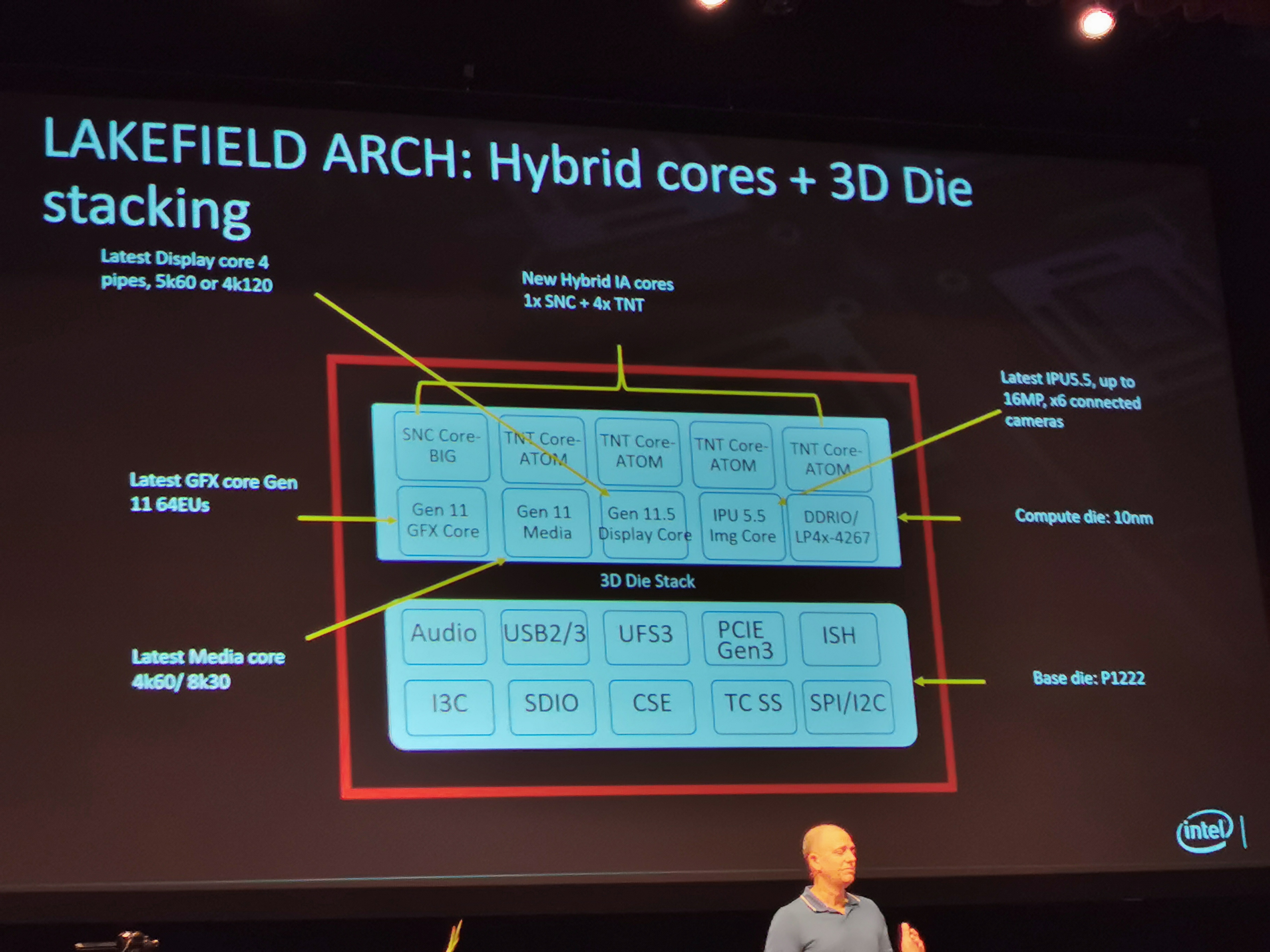
07:17PM EDT - We know a lot about Lakefield and Foveros: stacked logic and IO die, with POP DRAM. Hybrid x86 with 1x Sunny Cove and 4x Tremont
07:17PM EDT - This is the packaging session on Hot Chips, so we might learn more about the Foveros
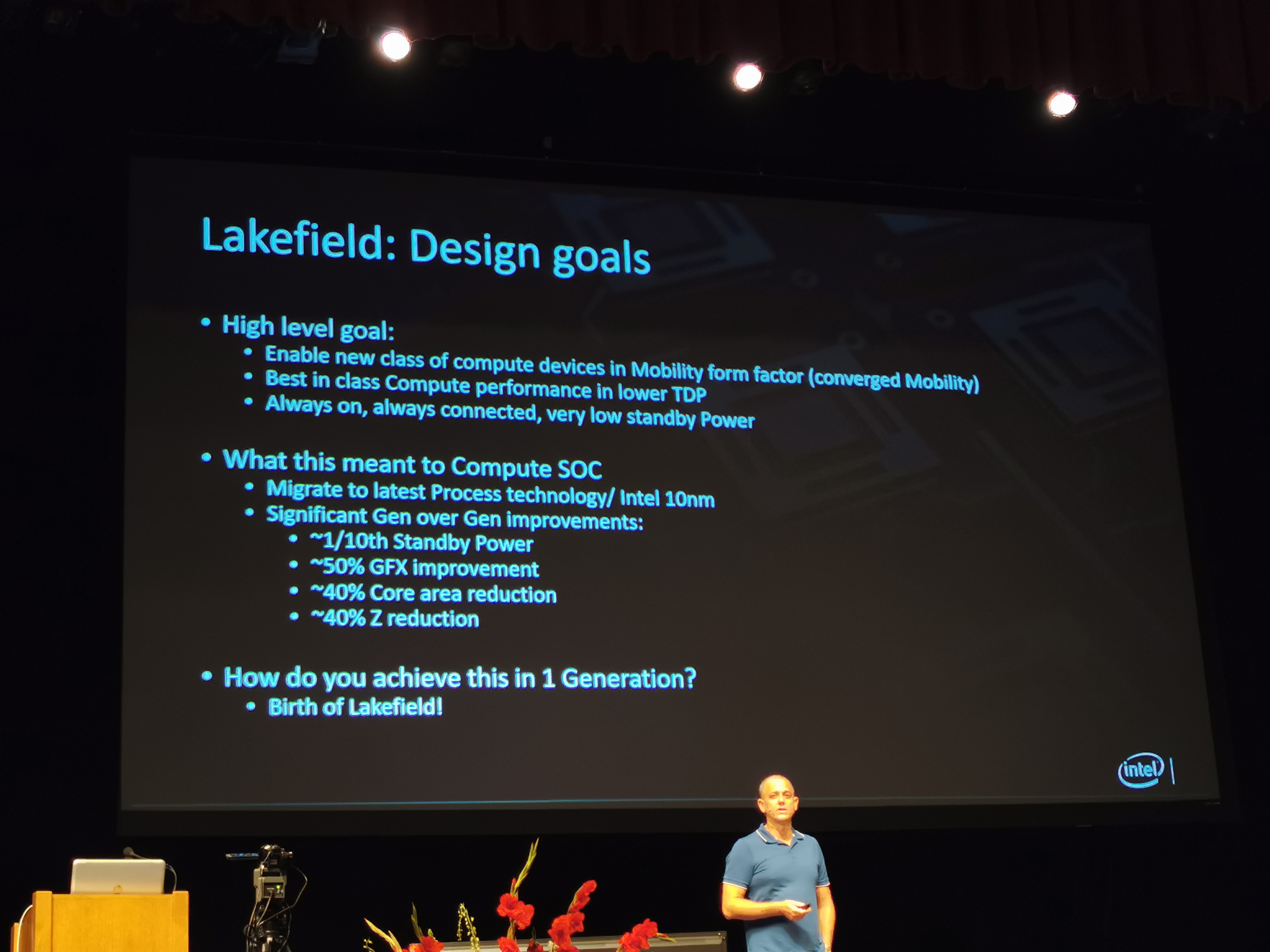
07:17PM EDT - Lakefield for smartphone and laptops
07:18PM EDT - Best in class compute in smaller form factor
07:18PM EDT - Customer request
07:18PM EDT - Lots of requirements, including 10nm and 2mW standby Power
07:19PM EDT - Also had to be small
07:19PM EDT - and high performance
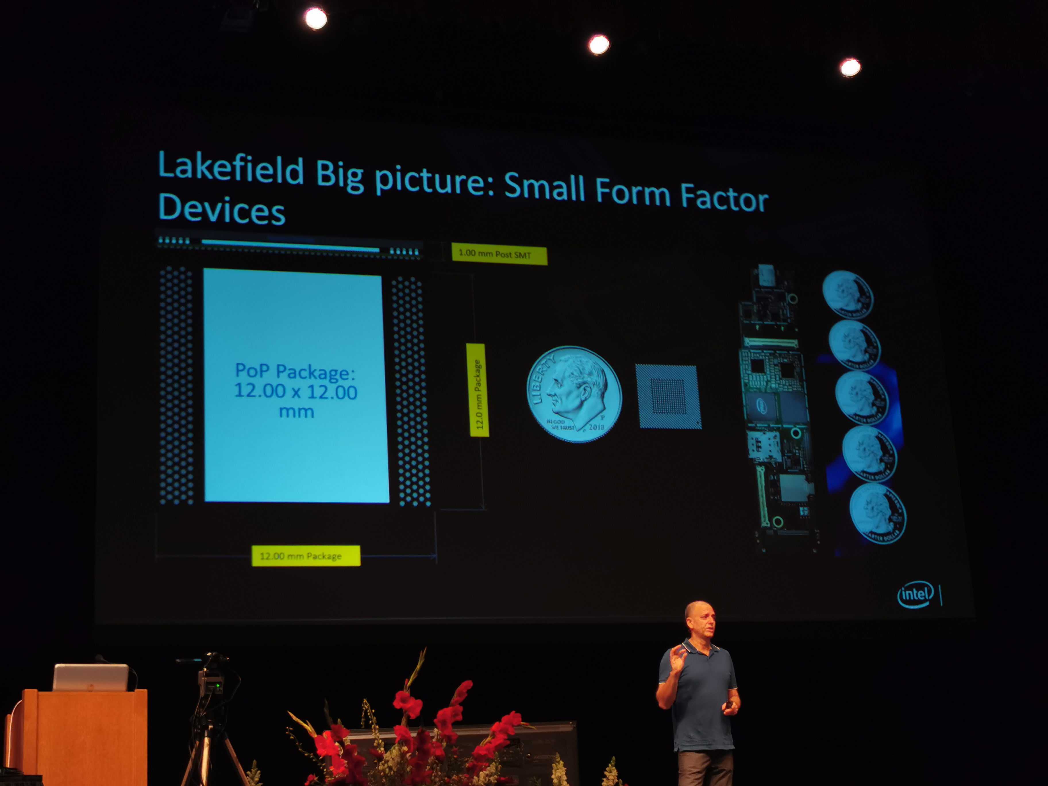
07:20PM EDT - Compute Die, base die, and 4GB (4 Gb?) memory on top
07:20PM EDT - 1mm z-height with post-SMT
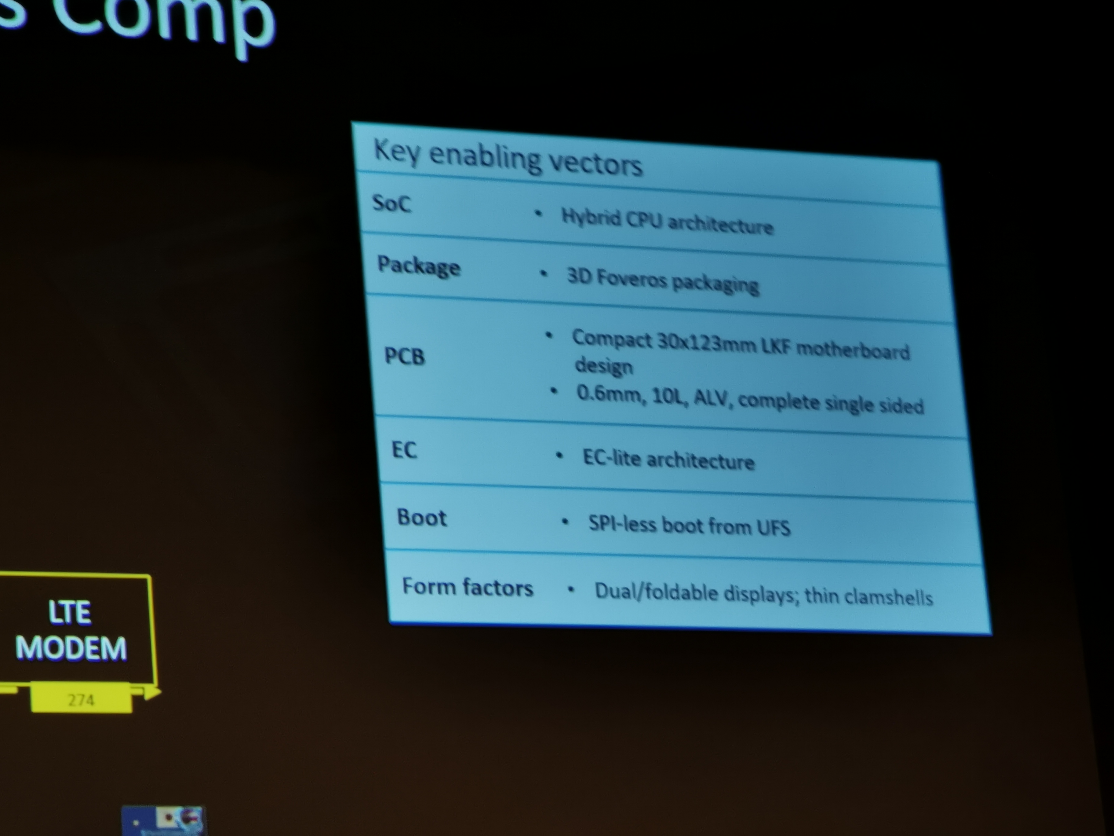
07:21PM EDT - 30x123 PCB for full compute on a PCB
07:21PM EDT - SMallest ever Intel complete solution
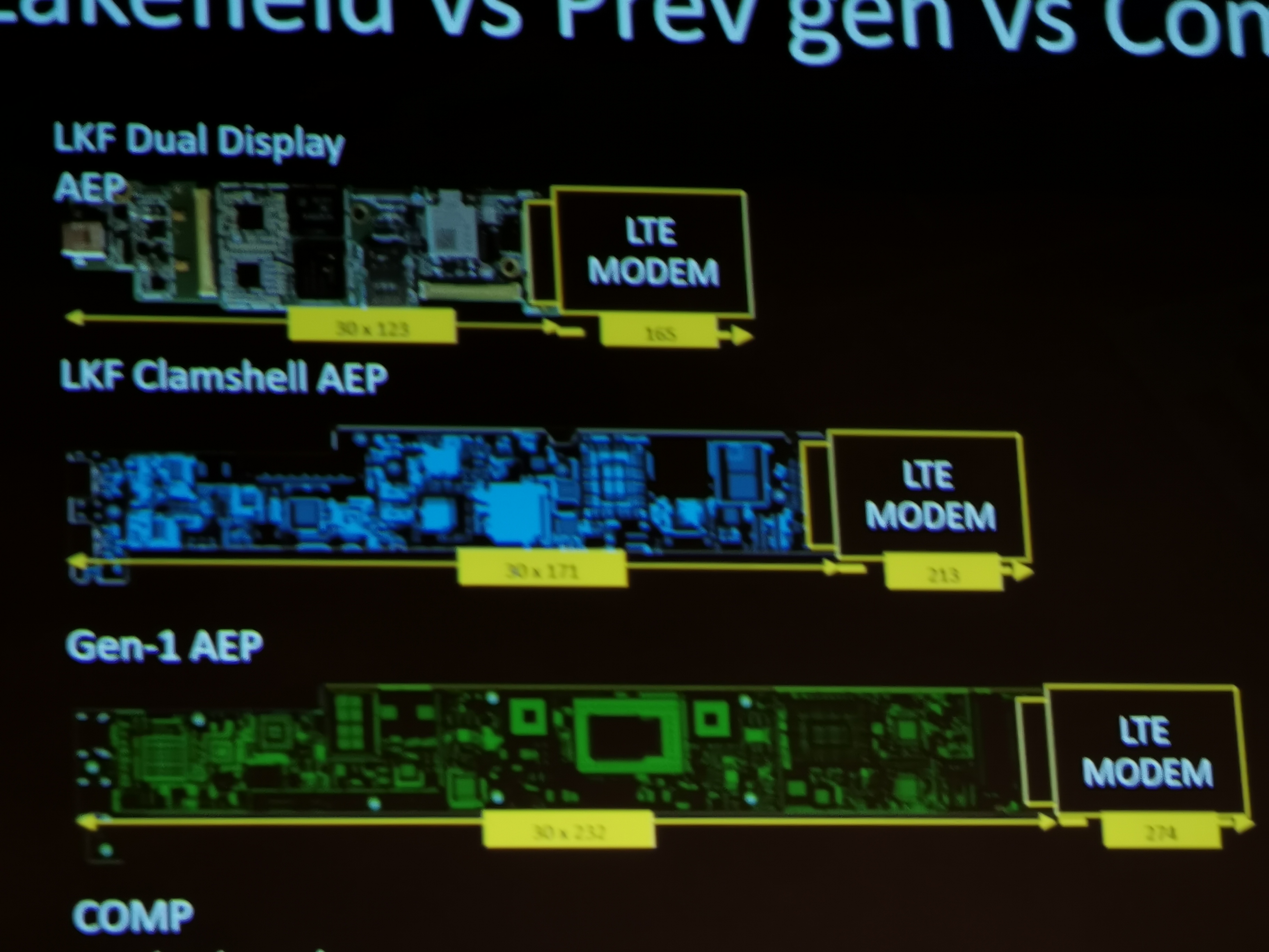
07:22PM EDT - Competitor PCB is 43x286 mm
07:22PM EDT - Competitor has onboard LTE modem, Intel does not
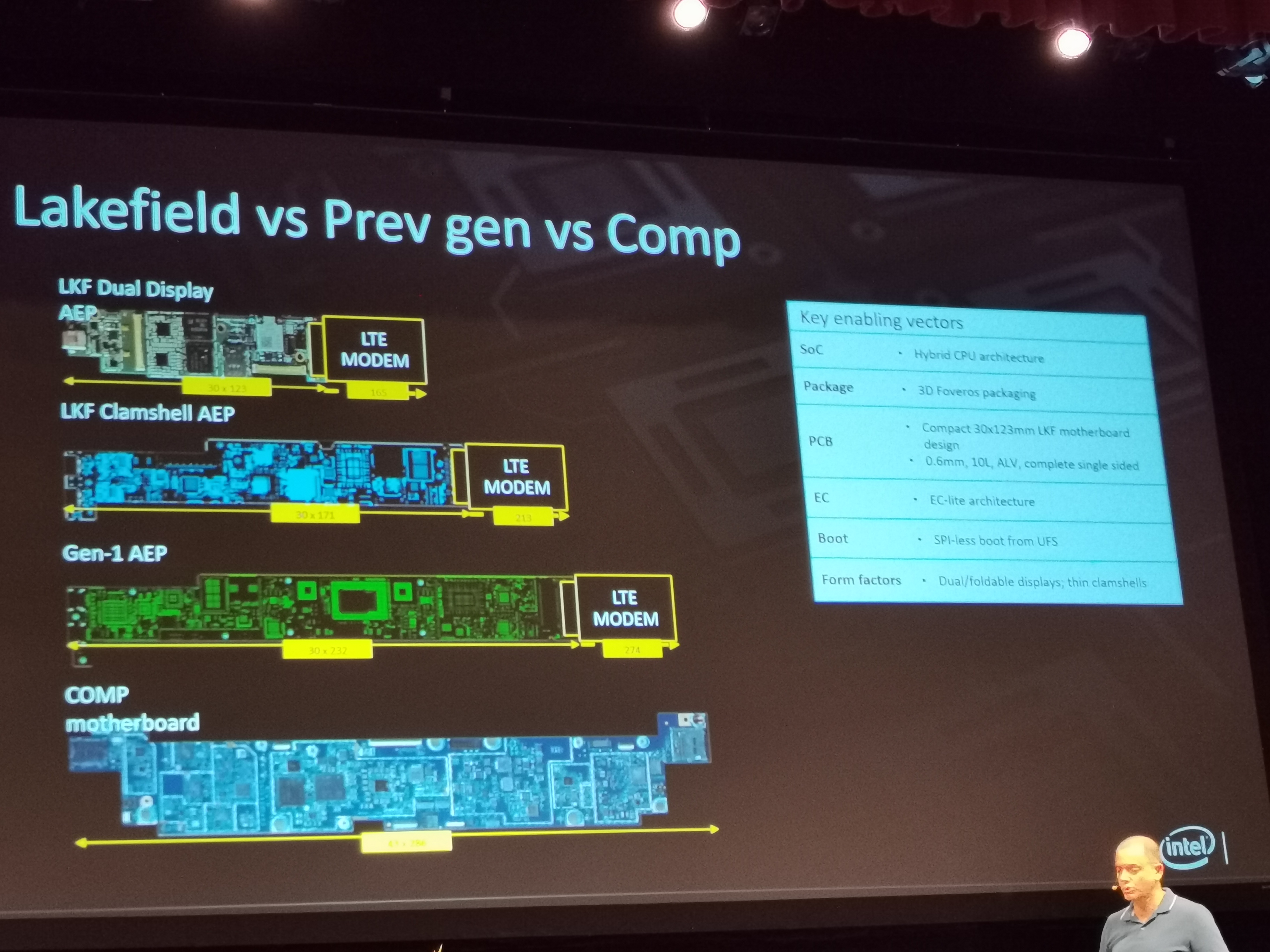
07:22PM EDT - LKF Clamshell AEP is what we'll see in notebooks
07:22PM EDT - PCB is 10 layer
07:23PM EDT - SPI-less boot from UFS
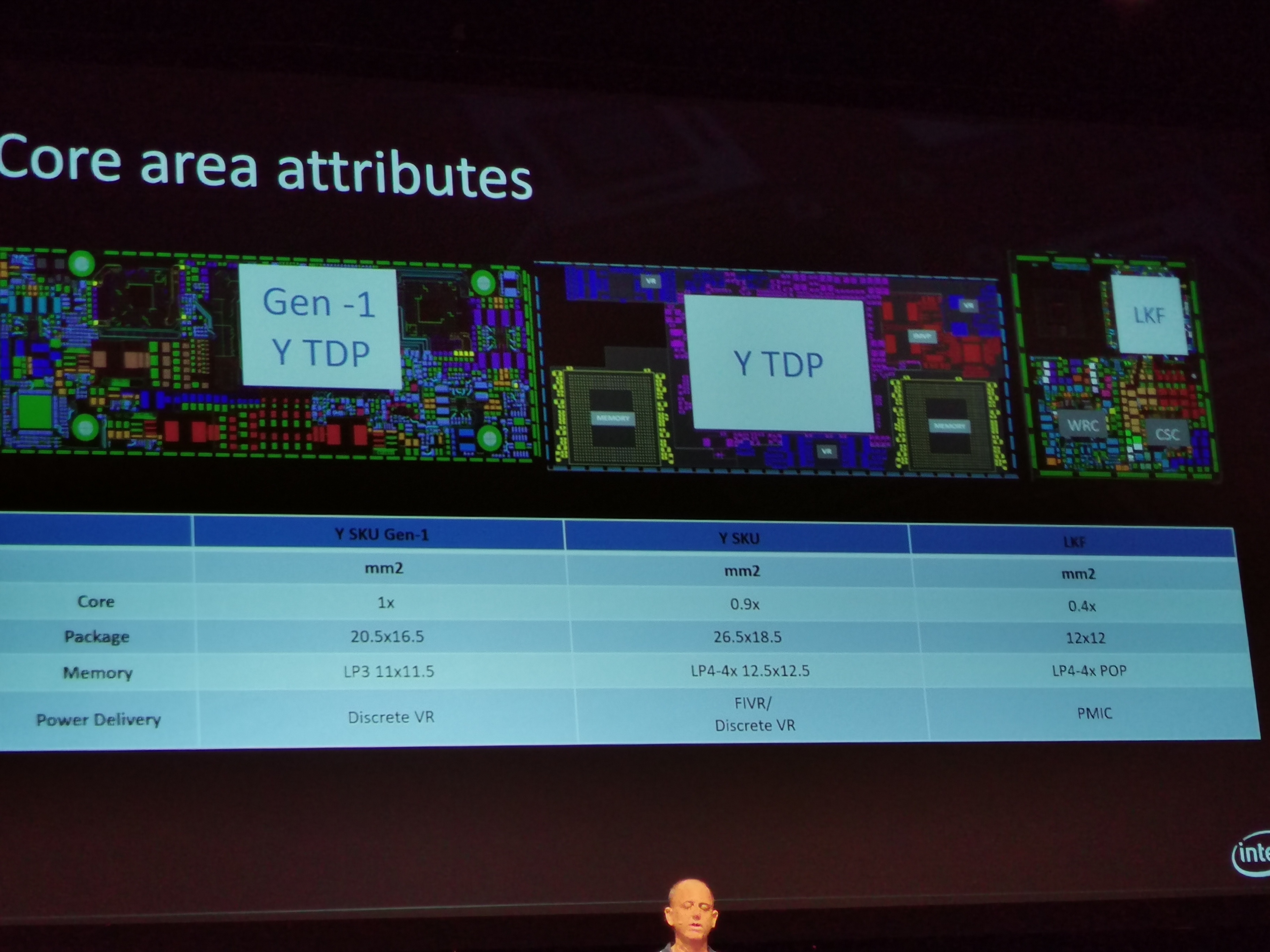
07:23PM EDT - Comparing last gen Y CPU vs LKF
07:24PM EDT - Amber vs Ice-Y vs Lakefield
07:24PM EDT - Power Delivery is PMIC
07:24PM EDT - Two PMICs in LKF, one for Compute die, one for IO die
07:25PM EDT - Compute in 10+
07:25PM EDT - (Once Again, the computer with the demonstration doesn't have the Intel font)
07:25PM EDT - 1x Sunny Cove + 4x Tremont
07:26PM EDT - Can support up to 6 cameras
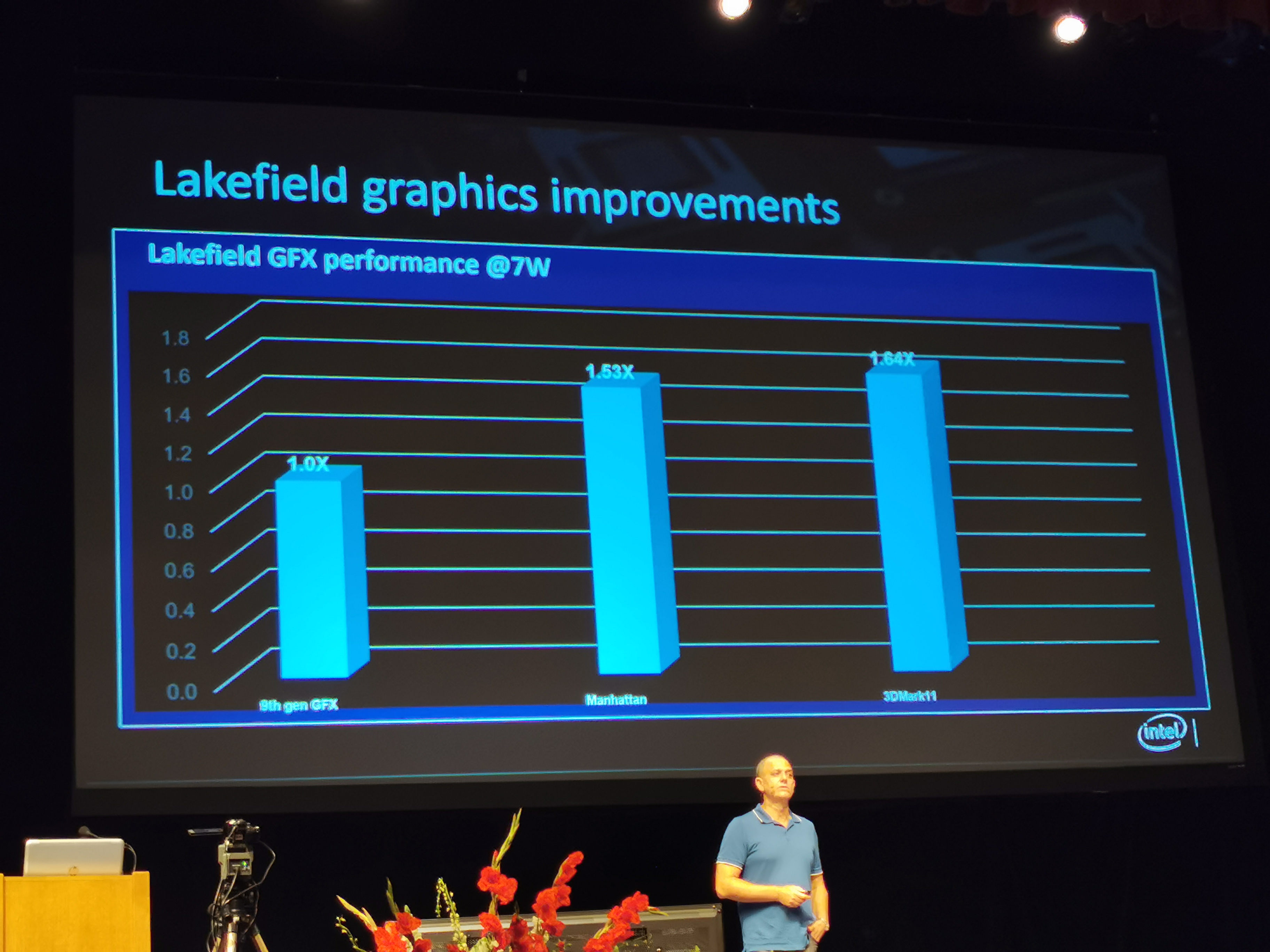
07:26PM EDT - Gen 11 graphics, 64 EUs
07:26PM EDT - Base Die is P1222
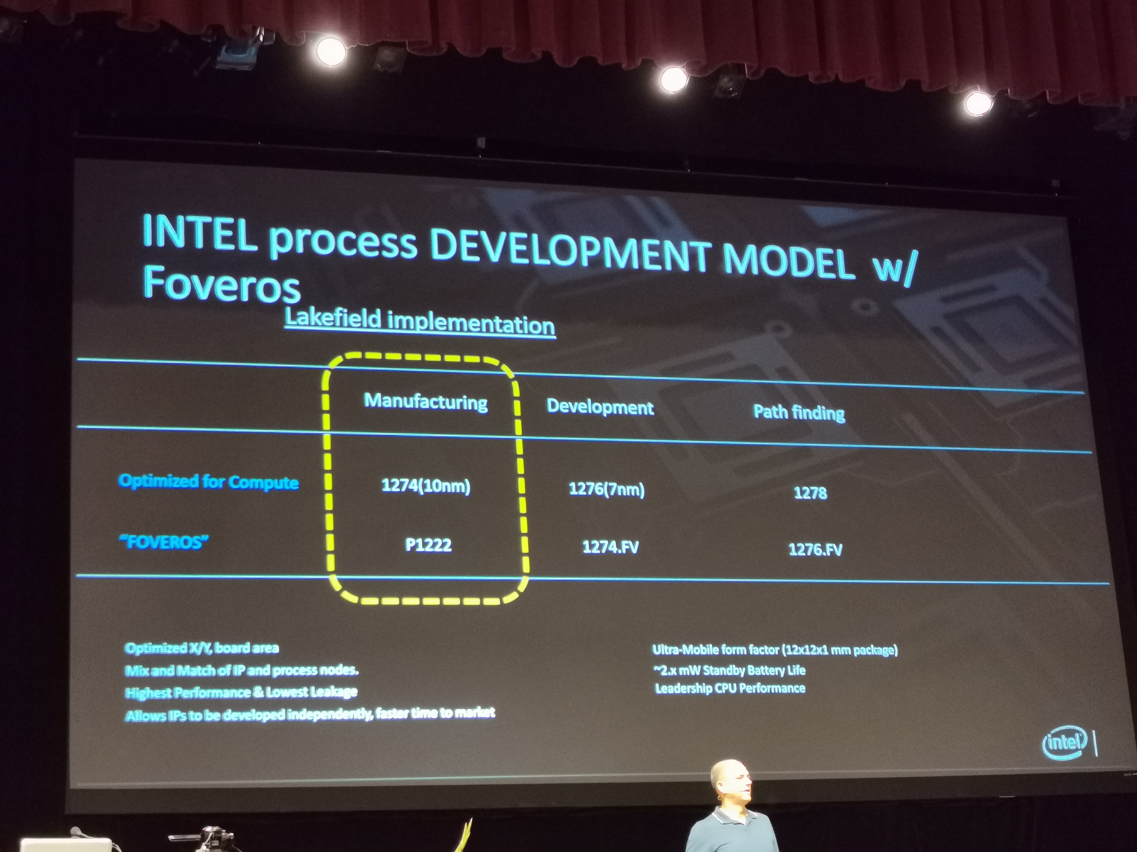
07:28PM EDT - P1222 is 10nm
07:28PM EDT - 7nm in development
07:28PM EDT - Sorry, P1222 isn't 10nm. it's 14nm
07:28PM EDT - Multi-die behaving like a monolithic die
07:29PM EDT - Allows IPs to be developed independently, faster time to market
07:29PM EDT - Plan to make many more stacked SoCs
07:30PM EDT - (This new slide doesn't even have a capital L for Lakefield)

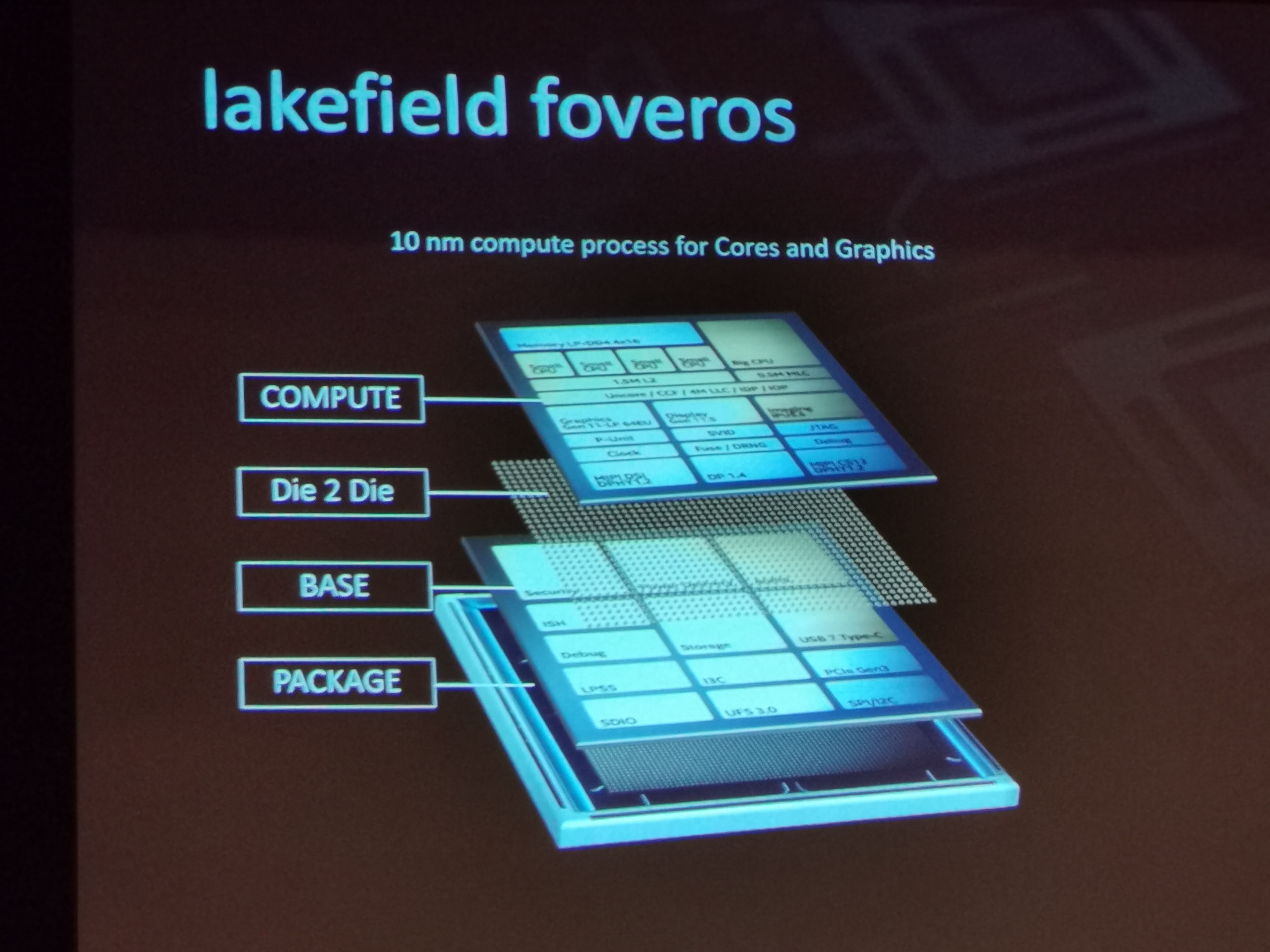
07:31PM EDT - 4 GB DRAM, or 8 GB LPDDR4X solution

07:31PM EDT - Now hybrid Compute
07:32PM EDT - Low power scenarios key to battery life run on Tremont
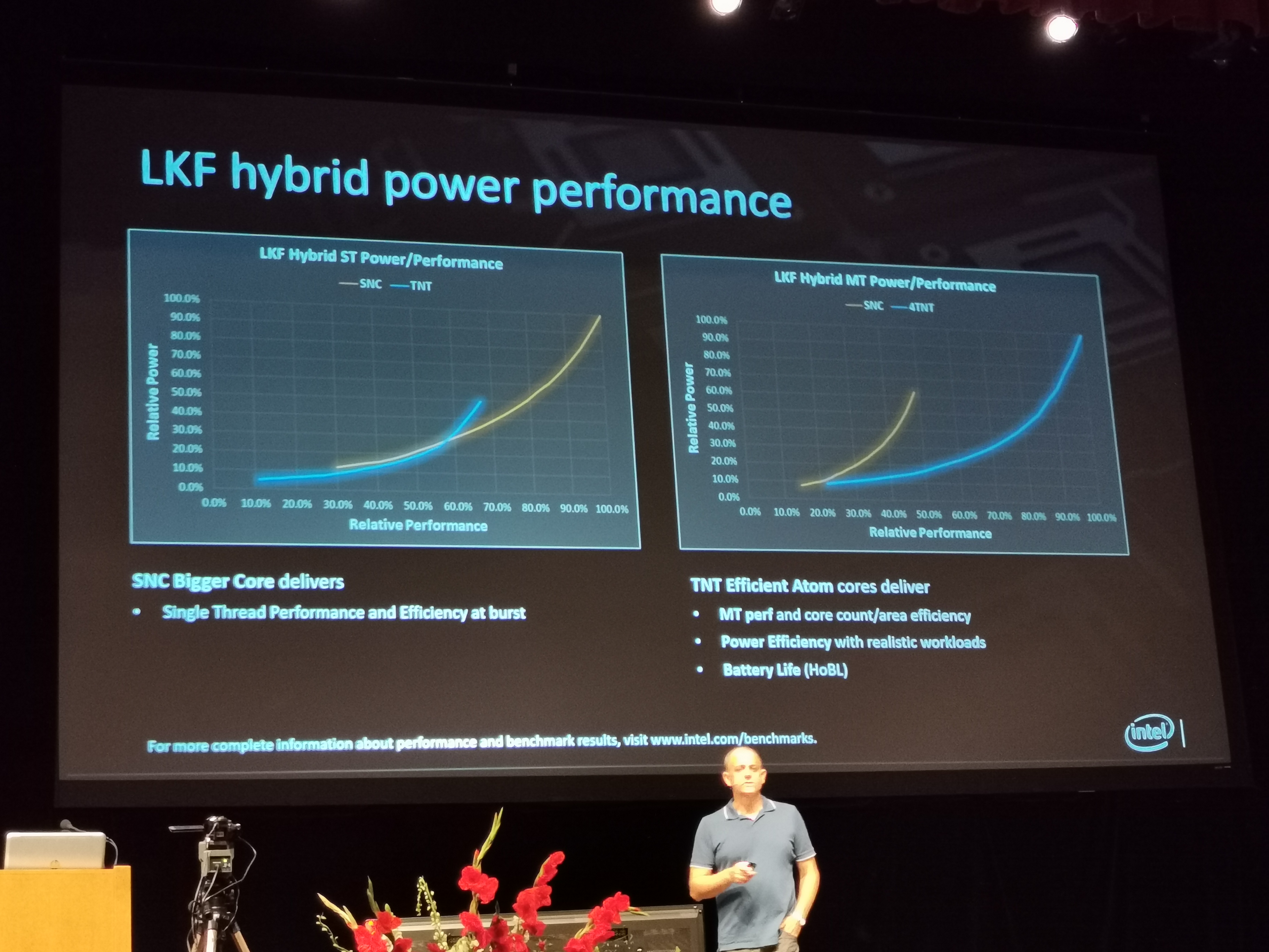
07:32PM EDT - There are power/perf curves for Sunny vs Tremont
07:33PM EDT - ST perf on SNC, low power on Tremont
07:34PM EDT - This slides also say it's better to run MT on Tremont
07:34PM EDT - So Sunny is only used for response-type latency workloads
07:34PM EDT - (What this means for multiple workloads running at the same time)
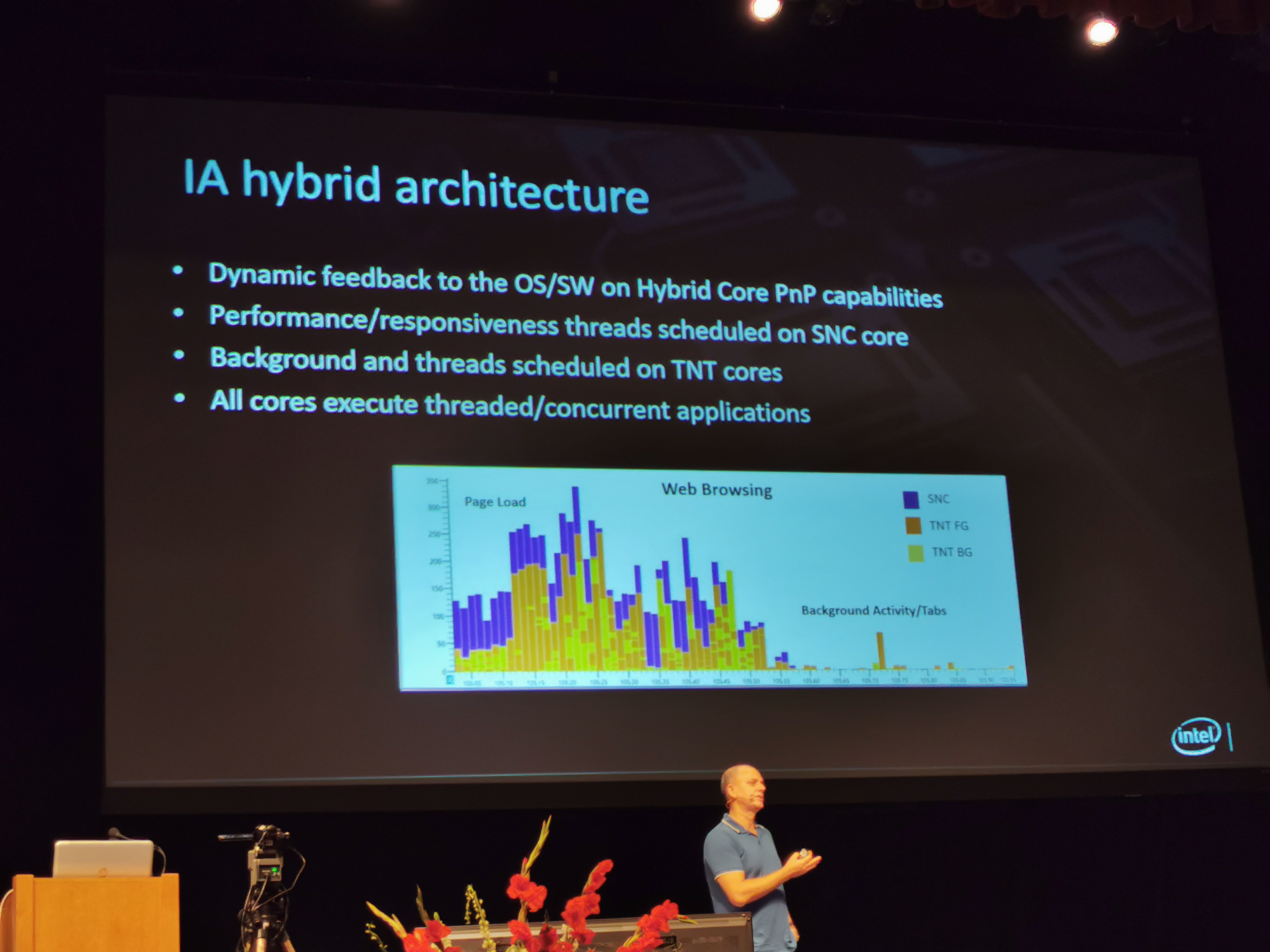
07:35PM EDT - (The person who made these slides really doesn't like capital letters in titles)
07:35PM EDT - Hybrid Architecture shows TNT as base, with SNC being run in specific sections
07:36PM EDT - Standby power is 0.08x over Skylake

07:37PM EDT - Vnn removal, LDO removal, low leakage power
07:37PM EDT - No need to use high perf transistors here. Can take advantage of low leakage transistors
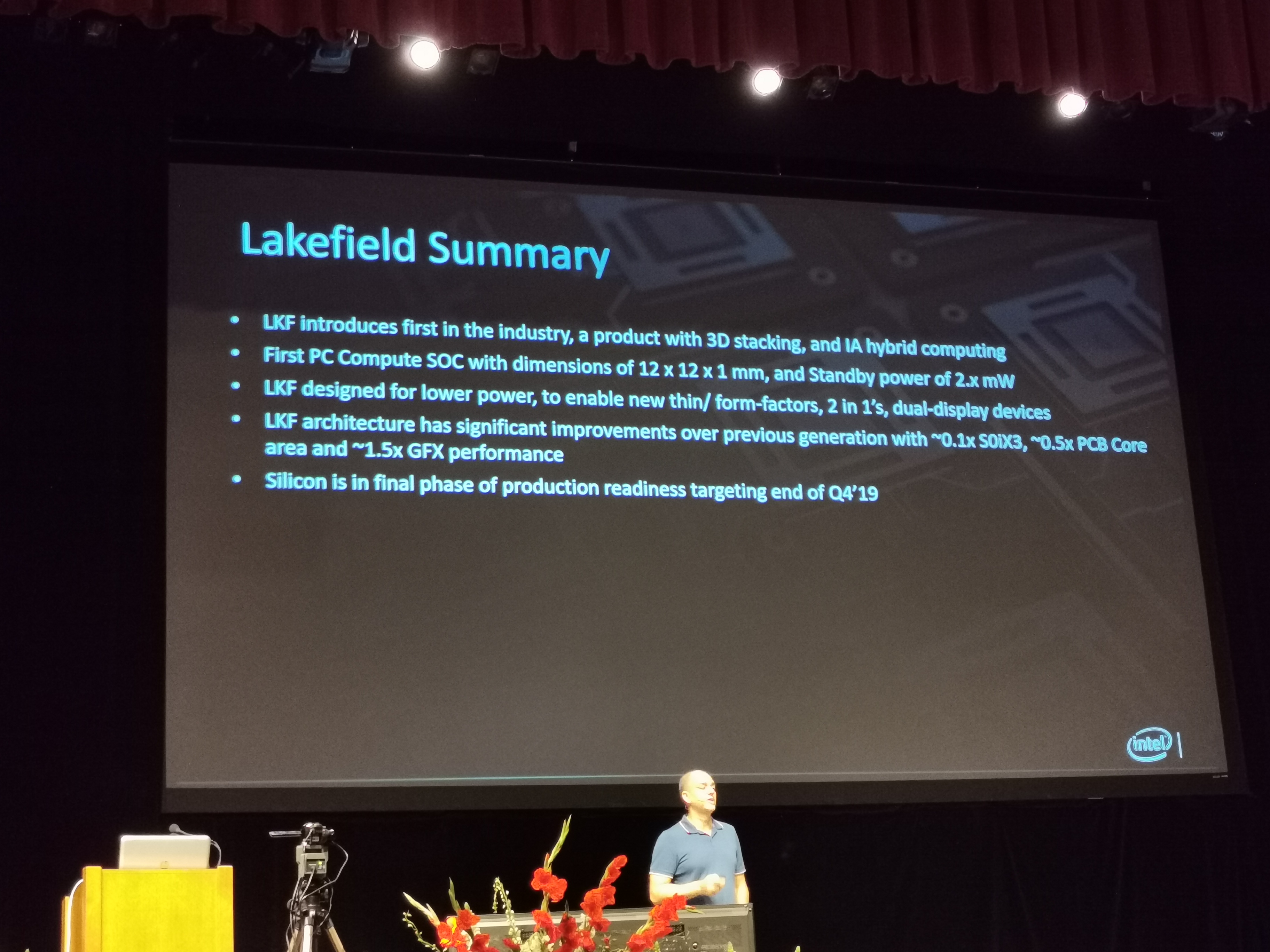
07:38PM EDT - First PC Compute SoC
07:38PM EDT - First phase of production, targeting readiness in Q4 2019
07:39PM EDT - Q&A?
07:39PM EDT - Q: Is it 10 or 10+? A: 10+
07:40PM EDT - Q: Interconnect between IO die and Compute die? A: Cut serialization and made it vertical
07:40PM EDT - Q: Face to face bonding of two dies? A: Yes
07:41PM EDT - Q: How is power and IO delivered through that connect? A: Combination of TSVs
07:42PM EDT - Q: pitch of microbumps? A: 50 micron pitch, 20 micron height
07:42PM EDT - Q: Can all the dies function independently or together? A: Can function independently like a normal PC
07:44PM EDT - Q: Penalty for keepaway from vias? A: The design rules are very forgiving - there are many classes of circuits that can be next to vias that can make it work. You won't use high speed, but on this product it was very easy to deliver.
07:45PM EDT - Q: Can you scale to higher power, with like a discrete GPU on top? How does that affect die rules? A: We don't see power limits, we think it will scan the entire range of the spectrum. Or the die to die scaling. It's a question of technology and ramping, then power delivery. It's all about working out the losses. We don't see a big limit from limiting 3D stacking.
07:46PM EDT - Q: Can you stack more dies? Thermals? A: Foveros is CoWoP with Silicon on Silicon, there should be no limit. Benefits of attaching many chiplets. Other pratical limits in architecture partitioning. Our goal is to drive it to many chiplets.
07:46PM EDT - That's a wrap. Now Xeon Jintide!


28 Comments
View All Comments
HStewart - Thursday, August 22, 2019 - link
Sunny Cove supports AVX 512 - not sure if that is included in core on Lakefield or TremontSantoval - Thursday, August 22, 2019 - link
It is certainly included (why would they redesign the Sunny Cove core just to remove the AVX-512 block?), but it might have been deactivated via firmware. Running AVX-512 code might blow up Lakefield's thermals well beyond 7W, unless perhaps the core was downclocked more than usual when running such code. The Tremont cores of course don't sport AVX-512, only the big Sunny Cove core might support it.name99 - Wednesday, August 28, 2019 - link
"Allows IPs to be developed independently, faster time to market"This is the kind of nonsensical statement that Intel KEEPS making that makes me so dubious about them. It sounds good --- until you start to think about it...
So we have a partition between compute and support functionality. OK, good.
And now I want to upgrade the support functionality, say from PCIe3 to PCIe4. OK, good.
So with Foveros I design the PCIe4 circuits, create the masks, fab the new support chip, great. That's a certain level of time and verification.
And suppose I was not using Foveros, but had a monolithic SoC. What would be involved?
I design the PCIe circuits, create the masks, fab the new chip, great. WHERE is the EXTRA time and verification? What's making the Foveros path a faster time to market?
The PCIe circuits, whether on the SoC OR on a separate die, should be isolated from the rest of the functionality by well defined interfaces. Modifying them should be no different whether the modifications are on a full SoC chip, or on a separate chiplet. Everyone else in the world understands this --- that's ARM's entire fscking business model, that they sell you certain functionality as separate items (cores, GPU, memory controller, etc) that you mix and match on the same SoC. And this works because: well defined interfaces that isolate functionality.
Which gets us back to the Intel comment. How can we interpret it?
- Intel has no clue how to isolate functionality on a SoC EXCEPT by putting it on separate chiplets. (Unlikely to be true, and terrifying if it is true...)
- Intel is flat out lying. This has zero to do with faster time to market (the rest of the world spins new SoCs, with massive upgraded functionality, every year -- doing so can be done if a company wants to do it). It's about, oh yes, 10nm yields. Keeping as much functionality as possible off 10nm as possible is necessary to ship anything in even small volumes.
Compare with AMD.
AMD has chiplets because
- it gives them optionality. They can sell a variety of different sizes, from 8 to 64 cores, without needing many different mask sets
- once they have that optionality, under those circumstances it makes sense to do things like upgrade the IO chiplet separately
But Intel isn't playing that game. They aren't providing optionality with a range of LakeFields that provide 1, 2, up to 8 different Sunny Cove cores. Neither are they at anything close to the size limits where it ranges from expensive to impossible to create larger SoCs.
It simply makes no sense to split a SoC in this way --- unless your process yield is abysmal...
name99 - Wednesday, August 28, 2019 - link
"What this means for multiple workloads running at the same time"Means that Intel REALLY cheaped out with providing only one large core...
The performance implications are going to be obvious from the very first reviews.
Which makes you wonder --- why?
The obvious conclusion is, once again, 10nm yield -- get that die size as small as possible! It's hard to know if that was the issue without being able to see the size of the SNC core relative to, eg, GPU.
The other possibility is thermals. If SNC is just not that awesome in terms of watts generated (which seems plausible given how ICL is OK, but nothing spectacular, in that regard) then maybe two SNC's just can't be sustained in Foveros --- which seems, uh, problematic going forward...
(Thermal issues may not doom 3D stacking generally. TSMC seem confident about this, and they have a history of being reliable in their predictions. But Intel are stuck with their particular 10nm process, their particular design methodology --- chasing frequency rather than IPC --- and their details for Foveros --- exactly how things are bonded, exactly what thermal conduits are provided; and Intel's specifics for all of these are not TSMC's specifics.)
jvl - Friday, August 30, 2019 - link
Is it Lakefield, lakefield or lake field? Or LKF?Sewell5N - Wednesday, September 4, 2019 - link
Thanks for sharing this information <a href="https://ifacetimeapp.com/">ifacetimeapp<...Sewell5N - Wednesday, September 4, 2019 - link
Thanks for sharing this information https://ifacetimeapp.com/Cherryparker - Monday, September 16, 2019 - link
I wish more authors of this type of content would take the time you did to research and write so well. I am very impressed with your vision and insight. i'll suggest you all to checkGeek Squad Support Phone Number visit https://www.errorcodeexpert.com/geek-squad-support... so you can resolve your all technical issue for home appliances or for a mac pro, television laptop etc.