SK Hynix Announces 3.6 Gbps HBM2E Memory For 2020: 1.8 TB/sec For Next-Gen Accelerators
by Ryan Smith on August 12, 2019 10:00 AM EST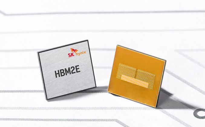
SK Hynix this morning has thrown their hat into the ring as the second company to announce memory based on the HBM2E standard. While the company isn’t using any kind of flash name for the memory (ala Samsung’s Flashbolt), the idea is the same: releasing faster and higher density HBM2 memory for the next generation of high-end processors. Hynix’s HBM2E memory will reach up to 3.6 Gbps, which as things currently stand, will make it the fastest HBM2E memory on the market when it ships in 2020.
As a quick refresher, HBM2E is a small update to the HBM2 standard to improve its performance, serving as a mid-generational kicker of sorts to allow for higher clockspeeds, higher densities (up to 24GB with 12 layers), and the underlying changes that are required to make those happen. Samsung was the first memory vendor to announce HBM2E memory earlier this year, with their 16GB/stack Flashbolt memory, which runs at up to 3.2 Gbps. At the time, Samsung did not announce a release date, and to the best of our knowledge, mass production still hasn’t begun.
Not to be left behind, SK Hynix is now also readying their own HBM2E memory. In terms of performance, SK Hynix says that their memory will be able to clock at up to 3.6 Gbps/pin, which would give a full 1024-pin stack a total of 460GB/sec of memory bandwidth, and in the process the lead for HBM2E memory speeds. And for more advanced devices which employ multiple stacks (e.g. server GPUs), this means a 4-stack processor could be paired up with as much as 1.84TB/sec of memory bandwidth, a massive amount by any measure. Meanwhile their capacity is doubling, from 8 Gb/layer to 16 Gb/layer, allowing a full 8-Hi stack to reach a total of 16GB. It’s worth noting that the revised HBM2 standard actually allows for 12-Hi stacks, for a total of 24GB/stack, however we’ve yet to see anyone announce memory quite that dense.
Given SK Hynix’s announcement, it’s interesting to note just how quickly HBM2 memory speeds have ramped up here: HBM2 vendors could barely do 1.9 Gbps 24 months ago, and now we’re looking at a near doubling of memory speeds in 3 years. This is a rather significant gain in a short period of time, especially with only a minor revision to the HBM2 spec being required. That said, I remain curious as to how SK Hynix (and Samsung) are going to deal with the heat of an 8-Hi stack running at those clocks; the HBM design philosophy is wide-and-slow, and 3.6 Gbps arguably isn’t so slow.
With their HBM2E memory set to go into mass production in 2020, SK Hynix expects the new memory to be used on “supercomputers, machine learning, and artificial intelligence systems that require the maximum level of memory performance.” All of these are distinctly high-end applications where HBM2 is already being heavily used today, so HBM2E is a natural extension to that market. At the same time, it’s also a reflection of the price/margins that HBM2 carries. HBM2 has remained (stubbornly) high-priced well after its release – a situation that memory manufacturers seem to be perfectly content with – and we’re not expecting HBM2E to change that. So expect to see SK Hynix’s HBM2E memory remain the domain of servers and other high-end equipment.
Source: SK Hynix


23 Comments
View All Comments
Yojimbo - Monday, August 12, 2019 - link
Actually memory bandwidth has been an issue for consumer GPUs for a while. Companies recognized it years ago and NVIDIA especially invested significant resources to help mitigate the problem. If the memory bandwidth had been there on the road map to begin with they would have used it and put the resources somewhere else. AMD have been bandwidth limited in the meantime because they didn't have the same resources to spend.zepi - Monday, August 12, 2019 - link
There might be benefits to be had in laptops for mid-range GPU's. Instead of 128bit GDDR5 / 6 they could use one stack of HBM2(E) to save space and power, which might be interesting for vendors like Apple & Microsoft, who can charge very high prices for their top-end mobile devices.Obviously it is not interesting for your $999 gaming laptop manufacturer who much rather increases the dimension of the mobo by couple of cm² to fit few more memory chips, but for Surface Book and Macbook pro models going for $2000+, increased energy efficiency and space savings (more battery) could be worth it.
quadrivial - Friday, August 16, 2019 - link
I actually think HBM solves a much more interesting problem than that. APU performance suffers a lot because CPUs need better latencies than GDDR6 provides while GPUs need higher bandwidth than DDR4 can provide. HBM has more bandwidth, lower latencies, AND lower power.A current stack of HBM supposedly costs around $80 per 4GB or around $20/GB. If new stacks can provide 2x the density, that price should reduce cost by 50% or more. That would make 16GB around $160 or around $185 with a $25 substrate. AMD can provide their current desktop APUs for $100 - $150. Doubling the GPU from 10CU to 20CU would increase die size roughly 30-50%.
For $400-450, I'd buy that chip.
rocky12345 - Monday, August 12, 2019 - link
GPU's at least on AMD's side are a bit BW starved On Vega 10 it is very clearly seen once you OC the HBM2 past stock and see a decent performance increase in most games. Navi 10 is somewhat starved as well but not to the same extent as Vega 10 is. There have been videos on YT where they have looked into this on Navi recently and found that at a certain point over clocking the core has little affect on speed and even the little bit of extra OC they got from the GDDR6 netted a decent amount of extra performance but it is to bad that the GDDR6 on Navi has so little room left for any kind of extra OC. My own thinking is that it might have someting to do with the GPU's IMC or maybe board design and that if it is just because of the way the boards are designed maybe the third party cards coming out that are custom cards will fix this problem hopefully.On my own Vega 56 bios flashed to 64 just going from 800MHz HBM2 to 945MHz HBM2 nets a huge performance gain and if you are lucky and the memory will go even higher like mine does 1150MHz sees another major step up for performance. It would be the same and probably to some extent even a bigger gain for the 64 at 1100-1150MHz HBM2.
ksec - Monday, August 12, 2019 - link
The reason why you are not seeing memory limitation is because GPU performance scales pretty much linearly with transistor count, and you only get transistor increase with die shrink.So for every die shrink, assuming the same die size and work load you will need an increase in memory bandwidth. Not to mention we need faster memory so less Die Space are used for I/O.
We have been stuck with 16/14nm for a long time. We have clear roadmap now for 7nm, 5nm, and 3nm for the next 5 years. Which means we need something like 3 - 5x more bandwidth, and as I mentioned I/O don't shrink as well as logic, at some point the cost of using HBM will be less than wasting Die Space on GDDR controller. ( Assuming HBM also drop in price )
azfacea - Monday, August 12, 2019 - link
what u r saying is percisely 100% flase. its quite the otherway around. nvidia and radeon cards are both memory bottlenecked at the moment and benefit immensly from memory overclocks. radeon was even more bw starved than nvidia. if u had any clue what radeon 7 was relative to vega 64, in terms of CU count Clocks and memory bw, u wouldnt have made this stupid comment.with higher res and refresh rates even more bw will be required
extide - Monday, August 12, 2019 - link
Interestingly enough, the first GDDR5 GPU (Radeon HD 4870) used 3.6Gbps GDDR5.Dragonstongue - Monday, August 12, 2019 - link
would be GREAT if when they say HBM etc will be X speed that when we see on GPU is at least this speed, AMD is a bit "worse" at least were for Vega (due to power limits) that HBM was not running "spec speed" as it would kill its PCI SIG specifications (i.e go past this, you lose license/kill computers)anyway, cool they make faster HBM less power etc, but, it not matter if no one uses at that speed/power, does it? ^.^
that being said, pretty sure the "next" Vega or whatever will use this new HBM is going to be crazy quick (no reason why should not be at least a chunk % "better"
systemBuilder33 - Monday, August 12, 2019 - link
HBM2 practically bankrupted AMD. No thanks!darkswordsman17 - Monday, August 12, 2019 - link
Where are you getting that from? They sold a ridiculous amount of Vega cards with HBM2. They lucked out a bit in that it was good for mining, but its also been good for their pro uses (which is the market that Vega was really targeted at, and Vega was developed with HBM in mind).