TSMC Announces Performance-Enhanced 7nm & 5nm Process Technologies
by Anton Shilov on July 30, 2019 6:00 PM EST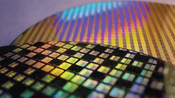
TSMC has quietly introduced a performance-enhanced version of its 7 nm DUV (N7) and 5 nm EUV (N5) manufacturing process. The company’s N7P and N5P technologies are designed for customers that need to make then 7 nm designs run faster, or consume slightly lower amount of power.
TSMC’s N7P uses the same design rules as the company’s N7, but features front-end-of-line (FEOL) and middle-end-of-line (MOL) optimizations that enable to either boost performance by 7% at the same power, or lower power consumption by 10% at the same clocks. The process technology is already available to TSMC customers, the contract maker of chips revealed at the 2019 VLSI Symposium in Japan, yet the company does not seem to advertise it broadly.
N7P uses proven deep ultraviolet (DUV) lithography and does not offer any transistor density improvements over N7. Those TSMC clients that need a ~ 18~20% higher transistor density are expected to use N7+ and N6 process technologies that use extreme ultraviolet (EUV) lithography for several layers.
While both N7 and N6 will be ‘long’ nodes that will be used for years to come, TSMC’s next major node with substantial density, power, and performance improvements is N5 (5 nm). The latter will also be offered in a performance-enhanced version called N5P. This technology will also feature FEOL and MOL optimizations in order to make the chips run 7% faster at the same power, or reduce consumption by 15% at the same clocks.
Related Reading:
- TSMC: Most 7nm Clients Will Transition to 6nm
- TSMC Reveals 6 nm Process Technology: 7 nm with Higher Transistor Density
- TSMC’s 5nm EUV Making Progress: PDK, DRM, EDA Tools, 3rd Party IP Ready
- TSMC: 7nm Now Biggest Share of Revenue
- TSMC: First 7nm EUV Chips Taped Out, 5nm Risk Production in Q2 2019
- TSMC Details 5 nm Process Tech: Aggressive Scaling, But Thin Power and Performance Gains
- Intel Details Manufacturing through 2023: 7nm, 7+, 7++, with Next Gen Packaging
Source: WikiChip.Org


36 Comments
View All Comments
Dragonstongue - Tuesday, July 30, 2019 - link
depends on how much "dark silicon" they must contend with and EVERYONE as they shrink further and further have to increase more and more (losing ground at they go further into making smaller)still dark silicon will make getting speed and actual performance very small % gains till at "best" Intel when they finally get to "true" 7nm after that it will be more of "how much regression can we handle while getting enough cores/cache to hide the dark silicon"
Nvidia might have pushed the speed way up for G 1xxx / RTX 2xxx however, their seeming "nitrous shot" is not going to be pushing the same frequency speed up as CPU did in years past (simpler design, also much simpler "do not pass go" walls because of such)
will be interesting to see the next 5 odd years as they are fast approaching the end of the silicon line (likely when optical come out and about for me and you, they will do similar "chiplet" so the stuff that not shrink well it at all can be kept in the "old but well known" shrinkage (lol) while the faster but more likely to get "dark silicon" they can only really use "wee bits and pieces"
I suppose, GPU and CPU folks might very well have to do what flash memory makers have done the last decade or what have you, SLC to MLC to TLC to QLC .. CPU/ GPU are more or less at the gap between MLC to TLC (happy spot where endurance and speed are meshing near perfect as is the cost for the capacity per wafer "cut" .. QLC on the other hand is "dark silicon" to keep my explain simple
QLC (much like cpu/gpu die shrink at this point) has very few advantages other than cost to produce (very little difference in cost for me and you) as well due to their "size they need to be" the capacity goes up (though performance drops significantly compared to the cost advantage i.e not much capacity/price advantage to really anyone vs "real world" usage (drop endurance a full 1/2 or more, few % less pricey .. seems more a way to get rid of crap wafers than viable drives (what do I know .. likely them makers not chuck anything in garbage if they find a way to make .01 become 100 ^.^
If we look at GPU .. 300mm/2 of today @ 12nm is something like 1200@ 65mn (something like that) so it seems "on paper" the newest fastest GPU/CPU are "fast" reality says they have just gotten far far better at "hiding deficits" (DDR4 higher bandwidth but more "sluggish" we as users only "see" the image painted, not being painted (i.e they get better at hiding or shifting the "deficit".
I honestly not see AMD really pushing to get 5+Ghz "all cores" as power use rises many times over going from 3-4Ghz, from 4-5 is WAY more power/heat even though was the same "% of increase" it is not a +1 = -1 scale .. +1 on speed might mean +15 power, minus 1 speed might mean save 5% power (they have very odd "sweet spots" though no one is immune from this, not Nvidia, not Intel, not IBM even (hell IBM had 5Ghz all core for a LONG TIME.. but, it cost a bunch of electricity and belch heat like crazy (9900k / Bulldozer / Pentium 965 ^.^
Santoval - Tuesday, July 30, 2019 - link
No it's not. TSMC's 5nm node will be even harder to reach clocks in the 4.8 to 5GHz range. Smaller features = higher leakage = more heat = lower clocks. TSMC's 2nd gen DUV 7nm node is different because apparently it is a highly optimized version of their original HP 7nm without increasing density at all. A Ryzen 9 3900X fabbed on that node could reach up to a single core 4.9 GHz boost clock with it.5 GHz boost clocks might have been possible with GAA-FETs (not in their original iteration, after they were quite optimized), but TSMC is not going to introduce GAA-FETs at 5nm. They will at 3/4nm, because at this scale FinFETs will completely run out of steam.
Santoval - Tuesday, July 30, 2019 - link
edit : Sorry, I thought you were referring to TSMC's 5nm node (too bad there is no edit option). TSMC at 7nm+ might reach higher clocks, but probably not in the 5 GHz range. It will depend on how much clocks they will gain from the EUV layers and how much they will lose from the 18 - 20% higher transistor density (it will be a balance between these two).name99 - Wednesday, July 31, 2019 - link
How come you're such an expert on TSMC 5nm capabilities that have not (as far as I can tell) been published? Where are you getting your "info" from?RSAUser - Thursday, August 1, 2019 - link
Same clock at a lower node would be higher IPC, I don't understand why people care about hitting 5GHz instead of pure performance numbers. 5GHz is a marketing spiel.deil - Wednesday, July 31, 2019 - link
I would opt for Ryzen 8 core with 35 TDPTeckk - Tuesday, July 30, 2019 - link
Is the 5nm process in HVM already? Considering it's on EUV and probably the first to get to that node, why do it silently then?Rudde - Wednesday, July 31, 2019 - link
5nm High performance is not at HVM yet.name99 - Wednesday, July 31, 2019 - link
It's in risk. None of this is silent, TSMC has been very open with the schedules.The schedule is basically identical to 7nm, shifted by two years. Which almost certainly means Apple will be on 5nm with 2020 A14, as the first large volume release.
A13 is likely on this 7nmP. (It's all somewhat unclear, but it seems like Apple is NOT using 7nm+, probably because of concerns that TSMC won't be able to provide the volumes Apple needs with its current amount of EUV equipment.)
AlbertS3 - Wednesday, July 31, 2019 - link
I just don't get it. The engineering is impressive but where is the benefit to the user. CPU technology using silicon hit the wall(s) many years ago and stalled at 4-5ghz. 12nm or 5nm performance is unchanged. 7nm and 5nm may reduce power for mobile devices but no performance gains for those of us with desktops. Intel once promised a 10ghz cpu - now a fairytale. Few single users will benefit from a 16, 32, or 64 core cpus. I see a lot of marketing hype with no real hope for any significant performance breakthroughs until we find a silicon replacement. Once found it may take a decade to reach consumers. Moore's law is long dead. Are we flogging a dead horse?