Intel Process Technology Update: 10nm Server Products in 1H 2020, Accelerated 7nm in 2021
by Anton Shilov on May 8, 2019 3:29 PM EST- Posted in
- Semiconductors
- Intel
- 10nm
- EUV
- 7nm
- Manufacturing
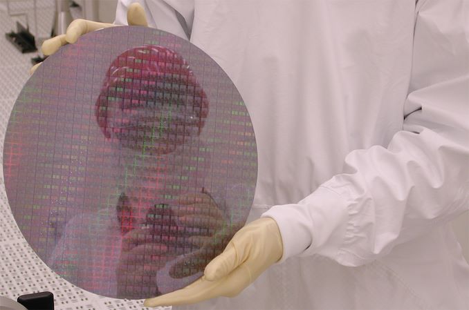
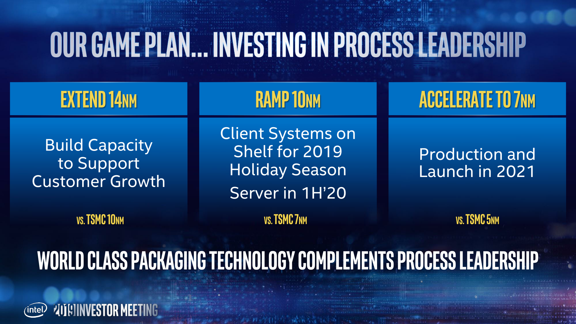
Intel provided an update regarding its upcoming fabrication technologies at its 2019 Investor Meeting. The company is on track to produce server-class products using its 10 nm manufacturing technology already in the first half of 2020, which is something that the company implied on for a while now, but never confirmed officially. What is relatively surprising is that Intel intends to start production of ccommercial chips using its 7 nm process already in 2021.
Intel’s 7 nm production technology had been in development independently from the 10 nm process and by a different crew, so this one is closer than one might think. The node is set to use extreme ultraviolet lithography (EUVL) with laser wavelength of 13.5 nm for select layers, so it will not heavily rely on multipatterning, a major source of problems with Intel’s 10 nm process. In fact, the use of EUV will simplify development of products, make it easier to produce them, and will likely shorten production cycle times too.
The first product to use Intel's 7 nm process technology will be Intel's Xe-architecture-based GP-GPU in 2021. The GPU will not only be made using Intel’s most advanced node, but will also us Intel’s Intel’s Embedded Die Interconnect Bridge (EMIB) technology as well as Foveros silicon stacking technique, which confirms that the product is not a monolithic design.
Speaking of non-monolithic designs, it is noteworthy that Intel considers its innovative chip packaging technologies no less important than its new nodes, so expect things like EMIB and Foveros to be a big part of Intel's future.
While Intel's first 7 nm product will be launched in 2021, Intel stresses that high-volume manufacturing (HVM) using the technology will begin in 2022 when the technology will be used not only for a server GPU, but also a server CPU. So, expect more 7 nm products three or four years down the road.

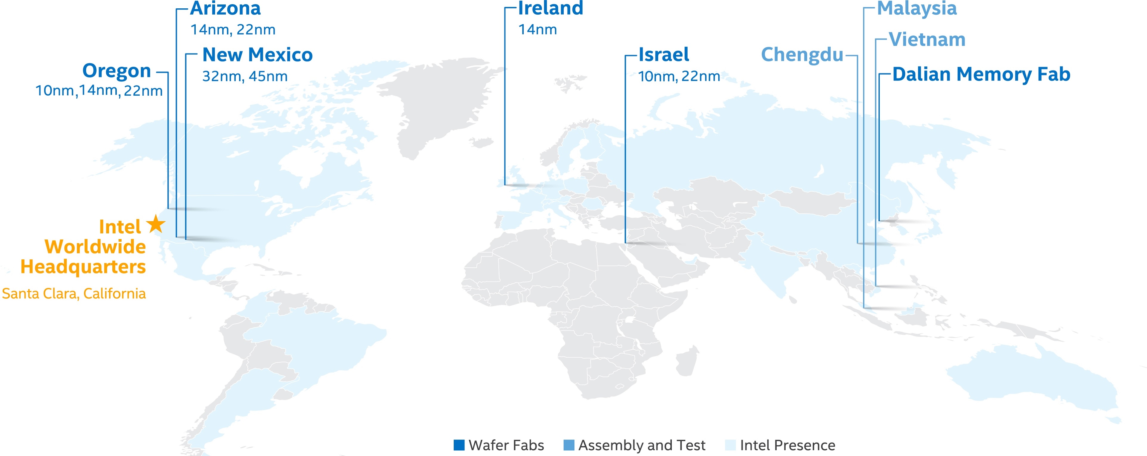
Late last year Intel announced a major plan to upgrade a number of its fabs for next-generation process technologies. Officially, Intel is equipping its Fab 42 in Arizona to make chips using its 7 nm fabrication process. Meanwhile, given the scope of Intel’s upgrade plan, which includes fabs in Oregon, Ireland, and Israel, it looks like the company might have other fabs ready for 7 nm by 2021 - 2022 timeframe.
Meanwhile, as Intel intends to refine all of its fabrication processes in the same manner as it did with its 14 nm node, expect Intel's 10 nm to co-exist with 7 nm for years.
Related Reading:
- Intel: EUV-Enabled 7nm Process Tech is on Track
- Intel Starts Qualification of Ice Lake CPUs, Raises 10nm Volume Expectation for 2019
- Intel Agilex: 10nm FPGAs with PCIe 5.0, DDR5, and CXL
- Intel to Equip Fab 42 for 7 nm
- Intel Discloses Plans to Spend $5 Billion on Fab 28 Expansion in Israel
- Intel Submits Ireland Fab Expansion Plan: $8 Billion Price Tag, With a 4 Year Lead Time
- Intel Details Plans for Its Oregon Fab Expansion: D1X Phase 3
- Intel to Expand Production Capacities at Multiple Fabs
Source: Intel


71 Comments
View All Comments
HStewart - Wednesday, May 8, 2019 - link
They only failed with Cannon Lake - all of the other stuff - is just BS on Internet.Wilco1 - Wednesday, May 8, 2019 - link
Or maybe you're the one with all the BS?eva02langley - Wednesday, May 8, 2019 - link
Remove your fanboy glasses. 10nm is a huge blow for Intel.name99 - Wednesday, May 8, 2019 - link
Actually no, the lies about great yields, shipping soon, started with Broadwell and 14nm. It's just that in that case the delay was "only" about 6..9 months, so the true believers could ignore then forget it.And remember it's not 10nm that has been the subject of constant lies. What about all those claims regarding Optane that have now been so aggressively scaled back? And 5G?
One error is reasonable, everyone makes mistakes or is too optimistic. But this is a clear pattern that's been going on for at least five years.
Korguz - Wednesday, May 8, 2019 - link
" They only failed with Cannon Lake - all of the other stuff - is just BS on Internet. " only failed with cannon lake ?? what about 10nm ??????? what about the fact.. that Epyc is on par.. or faster then Xeon when the software can use the cores it is given ?? the only BS that is there.. is the BS that you keep saying HStewart.. when will you wake up and realize your beloved intel.. is losing... failing.. and is falling behind... oh wait.. cause you cant, and you wont admit it..Kevin G - Wednesday, May 8, 2019 - link
Jumping to 7 nm is feasible considering the usage of EUV. This is what Intel should have done for 10 nm but EUV simply wasn't ready and they thought multipatterning could still scale. Sometime you make the wrong bet.The bigger news is that Xe will indeed be using EMIB. This opens the door for scaling between the low and high end by re-using the same piece of silicon, just numerous instances per package. This is something that should not be underestimated in terms of performance. With Intel having their own fabs, they can afford to throw far more silicon into the GPU race, more than even nVidia's insane 818 mm^2 monolithic die. The question is what size will the base Xe die be before they scale up in number? 300 mm^2? 400 mm^2?
name99 - Wednesday, May 8, 2019 - link
Why do you imagine that Intel is the only one with this sort of tech? As soon as it becomes appropriate, I expect nV and AMD to follow the same path (AMD already has, of course, with Ryzen).Packaging is currently undergoing an explosion of different possibilities. It's the shortest of short-sightedness to imagine that Intel's particular entries into this space (EMIB and Foveros) represent the only options, and that Samsung and TSMC have no clue about how to do this, or that their options inevitably suck compared to the Intel's...
Kevin G - Thursday, May 9, 2019 - link
Intel is the only one who also owns fabs. AMD and nVidia have access to other foundries but those are middle men who are out to make their share of money as well. The point is that Intel by merit of having their own fabs could throw more silicon into a product at a lower cost than either AMD or nVidia could. Intel could brute force their way to the performance crown which would be too costly for AMD or nVidia to match.The whole chiplet strategy for GPU is indeed being explored by both AMD and nVidia. There is a nice research paper published by nVidia on this very topic. AMD has strongly hinted at a similar concept for their future GPUs and CPU + GPU parts.
Irata - Thursday, May 9, 2019 - link
" This opens the door for scaling between the low and high end by re-using the same piece of silicon, just numerous instances per package"Um, isn't this exactly what AMD has been doing with Ryzen / Epyc / Threadripper in the CPU space for a while now ?
peevee - Thursday, May 9, 2019 - link
And Intel with Core 2 Quad 13 years ago.