Spotted: Qualcomm Snapdragon 8cx Wafer on 7nm
by Ian Cutress on December 6, 2018 4:35 PM EST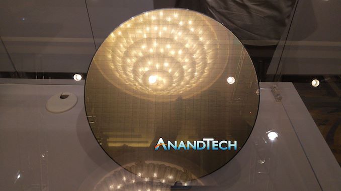
Alongside the announcement of the new 7nm Qualcomm Snapdragon 8cx processor for the company’s line of next generation premium tier Always Connected PCs, in the demo room today we saw a wafer of chips built on TSMC’s 7nm.
With this image, we can do one primary thing: work out the die size. Based on our estimates, we can see about 36 chips from top to bottom, and 22.2 chips from side to side. On a standard 300mm wafer, and give a little for the small amount of unused silicon from die to die so they can be cut up, we get a reasonable die size value of 112 square millimeters. This is what we expect to be the upper bound, and the final result may be lower.
That 112 mm2 is from a height of 8.3 mm and a width of 13.5 mm (which technically makes 112.05 mm2, but there is always margin for error here). This would make a total of 532 dies per wafer. There is no mention of defect rate or price per wafer in order to do an analysis of cost per die in manufacturing terms, but if ever get that information it would be an interesting metric.
In the slides, Qualcomm stated that the 8cx has double the transistors. We assume that’s a comparison to the Snapdragon 850, which is an overclocked S845, which had 5.3 billion transistors on the 10nm node. This would make the 8cx at around ~10 billion transistors (to 10.6b) at 112 mm2, or the equivalent of 89-95 million transistors per square millimeter (MTr/mm2). The Snapdragon 845/850 on 10nm would have been 56 MTr/mm2.
*It has come to our attention that the slide listing '2x transistors' was only referencing the size of the graphics of the chip, and not the whole chip itself. The table has been updated.
| Die Size and Transistor Counts | |||||
| AnandTech | Process Node | Die Size (mm) |
Die Area (mm2) |
Tr | Density (MTr/mm2) |
| Snapdragon 8cx | 7nm TSMC | 8.3 x 13.5 | 112* | > 5.3b < 10.6b |
> 56.4 < 94.6 |
| Snapdragon 845/850 | 10LPP Samsung | 94 | 5.3 b | 56.4 | |
| Snapdragon 835 | 10LPE Samsung | 72.3 | 3.0 b | 41.5 | |
| Kirin 980 | 7nm TSMC | 74.13 | 6.9 b | 93.1 | |
| Kirin 970 | 10nm TSMC | 9.75 x 9.92 | 96.72 | 5.5 b | 56.9 |
| Kirin 960 | 16nm TSMC | 10.77 x 10.93 | 117.72 | 4.0 b | 34.0 |
| Apple A12 Bionic | 7nm TSMC | 9.89 x 8.42 | 83.27 | 6.9 b | 82.9 |
| Exynos 9810 | 10LPP Samsung | 10.37 x 11.47 | 118.94 | ? | ? |
| 8-core Ryzen | 14nm GloFo | 22.06 x 9.66 | 192 | 4.8 b | 25.0 |
| Skylake 4+2 | 14nm Intel | 13.31 x 9.19 | 122 | 1.75 b | 14.3 |
| *Upper Bound | |||||
More information as we get it.


15 Comments
View All Comments
Santoval - Friday, December 7, 2018 - link
That number is indeed *way* too low. Intel has quoted 37.5 MTr/mm^2 for their 14nm process (and 2.7 times more for their 10nm process, i.e. ~101 MTr/mm^2). The relevant diagram -along with other comparisons of 14nm to 10nm- is in this pdf file, on the second page :https://newsroom.intel.com/newsroom/wp-content/upl...
name99 - Friday, December 7, 2018 - link
Transistors (and more generally cells, and then entire designs) come in at least two forms - density optimized and frequency (ie speed/performance) optimized.The high intel density numbers (like that 100MTr/mm^2) refer to density optimized designs. The problem is --- that's irrelevant to most of what Intel ships. Sure it's probably relevant to Atom, but when you think Intel, you think i7 or Xeon, you don't think Atom.
The density numbers for frequency optimized designs are lower on every process, but seem especially so on Intel.
edzieba - Monday, December 10, 2018 - link
Intel mix transistor densities within the same die. Cores can use freq-opt transistors while uncore can use dense-opt.Wilco1 - Friday, December 7, 2018 - link
Transistor density of Intel CPUs has always been bad, hence all the marketing hype. No Intel chips can even achieve half their claimed marketing density!See eg. https://www.anandtech.com/show/9582/intel-skylake-... or https://en.wikipedia.org/wiki/Transistor_count for many more datapoints.
The 22 core Broadwell E5 at ~15.8MTr/mm^2 gets about 40% the claimed 37.5MTr/mm^2 - most other Intel cores do around 13-14, or about a third the claimed density. Ryzen and Epyc achieve almost twice the density at 25MTr/mm^2. Note though that POWER 9 gets 11.5 on essentially the same process.
Why is this the case? Both IBM and Intel use huge transistors to squeeze out every bit of performance, so density suffers badly. On the other hand AMD proves one can achieve 4+GHz at almost twice the density.
This huge deficit in density was the reason Intel pushed density too far too quickly with 10nm (and 7nm) "hyperscaling". When 10nm finally goes to production it will likely have a far less ambitious density.
nismotigerwvu - Friday, December 7, 2018 - link
Moore's Law is a crazy thing. I remember being floored when AMD built the first gen Bulldozer chips from 1.2 billion transistors and now we have MOBILE SoCs packing nearly 5 fold more into a tiny die that draws 50 times less power.