Arm's Cortex-A76 CPU Unveiled: Taking Aim at the Top for 7nm
by Andrei Frumusanu on May 31, 2018 3:01 PM EST- Posted in
- CPUs
- Arm
- Smartphones
- Mobile
- SoCs
- Cortex-A76
Cortex A76 µarch - Frontend
Starting off with a rough overview of the Cortex A76 microarchitectural diagram we see the larger functional blocks. The A76 doesn’t look too different than other Arm processors in this regard and the differences come only with details that Arm is willing to divulge. To overly simplify it, this is a superscalar out-of-order core with a 4-wide decode front-end with 8 execution ports in the backend with a total implementation pipeline depth of 13 stages with the execution latencies of a 11 stage core.

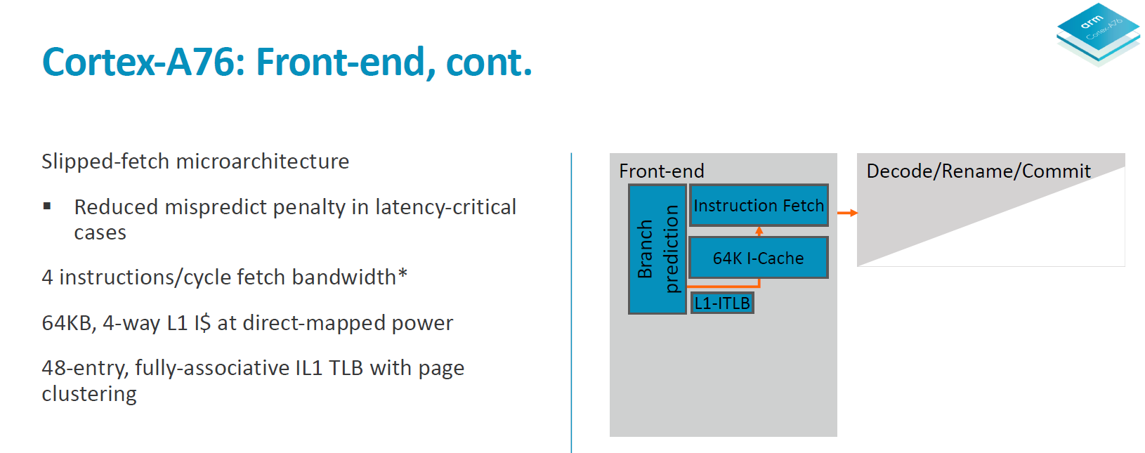
In the front-end, Arm has created a new predict/fetch unit that it calls a “predict-directed fetch”, meaning the branch prediction unit feeds into the instruction fetch unit. This is a divergence from past Arm µarches and it allows for both higher performance and lower power consumption.

The branch prediction unit is what Arm calls a first in the industry in adopting a hybrid indirect predictor. The predictor is decoupled from the fetch unit and its supporting large structures operate separate from the rest of the machine – likely what this means is that it will be easier to clock-gate during operation to save on power. The branch predictor is supported by 3-level branch target caches; a 16-entry nanoBTB, a 64-entry microBTB and a 6000 entry main BTB. Arm claimed back in the A73 and A75 generations of branch predictors were able to nearly predict all taken branches so this new unit in the A76 seems to be one level above that in capability.
The branch unit operates at double the bandwidth of the fetch unit – it operates on 32B/cycle meaning up to 8 32b instructions per cycle. This feeds a fetch queue in front of the instruction fetch consisting of 12 “blocks”. The fetch unit operates at 16B/cycle meaning 4 32b instructions. The branch unit operating at double the throughput makes it possible to get ahead of the fetch unit. What this serves is that in the case of a mispredict it can hide branch bubbles in the pipeline and avoid stalling the fetch unit and the rest of the core. The core is said to able to cope with up to 8 misses on the I-side.
I mentioned at the beginning that the A76 is a 13-stage implementation with the latency of an 11-stage core. What happens is that in latency-critical paths the stages can be overlapped. One such cycle happens between the second cycle of the branch predict path and the first cycle of the fetch path. So effectively while there’s 4 (2+2) pipeline stages on the branch and fetch, the core has latencies of down to 3 cycles.
On the decode and rename stages we see a throughput of 4 instructions per cycle. The A73 and A75 were respectively 2 and 3-wide in their decode stages so the A76 is 33% wider than the last generation in this aspect. It was curious to see the A73 go down in decode width from the 3-wide A72, but this was done to optimise for power efficiency and “leanness” of the pipeline with goals of improving the utilisation of the front-end units. With the A76 going 4-wide, this is also Arms to date widest microarchitecture – although it’s still extremely lean when putting it into juxtaposition with competing µarches from Samsung or Apple.
The fetch unit feeds a decode queue of up to 16 32b instructions. The pipeline stages here consist of 2 cycles of instruction align and decode. It looks here Arm decided to go back to a 2-cycle decode as opposed to the 1-cycle unit found on the A73 and A75. As a reminder the Sophia cores still required a secondary cycle on the decode stage when handling instructions utilising the ASIMD/FP pipelines so Arm may have found other optimisation methods with the A76 µarch that warranted this design decision.
The decode stage takes in 4 instructions per cycle and outputs macro-ops at an average ratio of 1.06Mops per instruction. Entering the register rename stage we see heavy power optimisation as the rename units are separated and clock gated for integer/ASIMD/flag operations. The rename and dispatch are a 1 cycle stage which is a reduction from the 2-cycle rename/dispatch from the A73 and A75. Macro-ops are expanded into micro-ops at a ratio of 1.2µop per instruction and we see up to 8µops dispatched per cycle, which is an increase from the advertised 6µops/cycle on the A75 and 4µops/cycle on the A73.
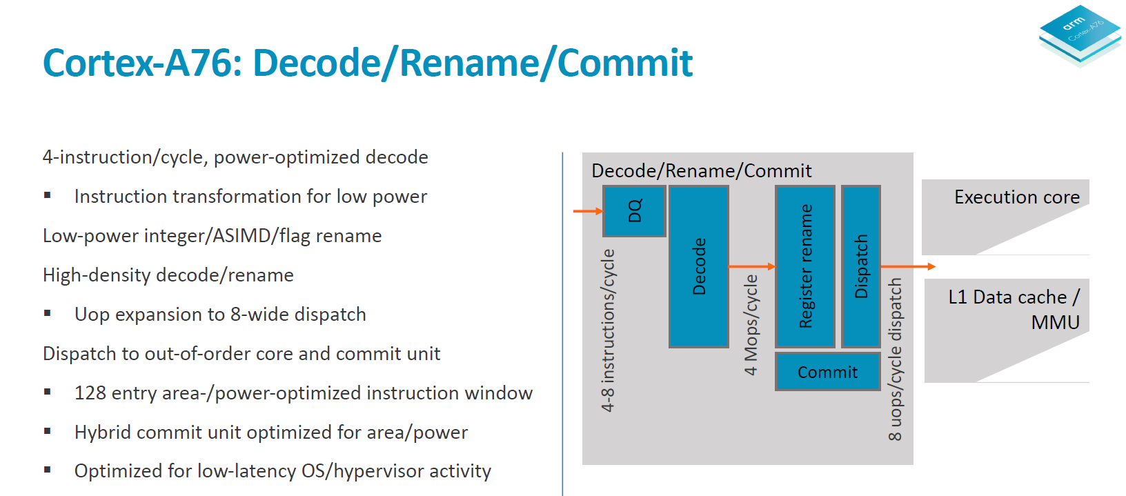
The out-of-order window commit size of the A76 is 128 and the buffer is separated into two structures responsible for instruction management and register reclaim, called a hybrid commit system. Arm here made it clear that it wasn’t focusing on increasing this aspect of the design as it found it as a terrible return on investment when it comes to performance. It is said that the performance scaling is 1/7th – meaning a 7% increase of the reorder buffer only results in a 1% increase in performance. This comes at great juxtaposition compared to for example Samsung's M3 cores with a very large 224 ROB.
As a last note on the front-end, Arm said to have tried to optimised the front-end for lowest possible latency for hypervisor activity and system calls, but didn’t go into more details.


123 Comments
View All Comments
serendip - Thursday, May 31, 2018 - link
Does anyone actually use the full performance of the A11 or A12 in daily tasks? To me, it's pointless to have a power hungry and fast core just for benchmarks. Just make a slightly slower core with less power usage for quick bursts like app loading or Web page rendering, while much slower and more efficient cores handle the usual workload.jOHEI - Thursday, May 31, 2018 - link
ARM's objectives is to make CPU's that go into a cluster of 4+ another 4 small ones.What Apple has does is Making bigger cores >2 times the size of an ARM core and have 1.5x the performance of the Said core. That same CPU is made for very high Power consumption at maximum load and Apple tweaks the ammount of time it stays in those high clocks. Thus its easier to make a laptop chip-tablet and phone. Because you just reuse the same CPU for all of them, maybe add a few cores to the laptop version and tweak the power settings and its relatively easy.
jOHEI - Thursday, May 31, 2018 - link
Forgot to mention that Apple goes for 2 core clusters, not 4. So they must have significantly better single core performance to matchup against the Conpetition.name99 - Friday, June 1, 2018 - link
Just to correct that you are somewhat living in the past with your numbers.ARM no longer cares about 4-sized clusters; that was an artifact of big.LITTLE (and one of the constraints that limited that architecture's performance). The successor to big.LITTLE, brand-named dynamIQ, does not do things in blocks of 4 anymore.
Likewise Apple first released 3 CPUs in a SoC with the A8X. The A10X likewise has three CPUs. It's entirely likely (though no-one knows for sure) that the A11X (or A12X if the 11X is skipped) will have 4 large cores.
BurntMyBacon - Friday, June 1, 2018 - link
Due to ARM's licensing model, they have every incentive to push designs that cater to more cores. They have little incentive to push single threaded performance any more than necessary as this would result in few cores being licensed due to space and power constraints. I'm not fully convinced that the whole big.LITTLE (and derivative) philosophy was the best way to go either. It could be that it got close enough to what advanced power management could do with the benefit of providing a convincing case for ARM CPU designers to use double the cores or more. When Intel was still in the market, they demonstrated that a dual core chip with clock gating, power gating, power monitoring, dynamic voltage and frequency scaling, and other advanced power management features could provide superior single thread performance and comparable multithread performance in a similar power envelop to competing ARM designs with double the cores (all while burdened with the inefficient x86 decoder). Apple also had good success employing a similar philosophy until their A10 design. Though, it is not necessarily causal, it is interesting to note that they've had more trouble keeping within their thermal and power constraints on their latest A11 big.LITTLE design.Note: I don't have any issue with asymmetric / heterogeneous CPUs. I'm just not convinced that they are adequate replacements for good power management built into the cores. DynamIQ does seem to be a push in the right direction allowing simultaneous usage of all cores, providing hooks for accelerators, and providing fine grained dynamic voltage and frequency scaling. This makes a lot of sense when you can assign tasks to processors (or accelerators) with significantly better proficiency for the task in question. Switching processors for no other reason than it is lower power, however, just sounds like the design team had no incentive to further optimize their power management on the high performance core.
name99 - Friday, June 1, 2018 - link
Again a correction.Apple's problems with the A10 and A11 are NOT problems of power management; they are problems of CURRENT DRAW. Power management on the chips works just fine (and better than ever; high performance throttling tends to occur less with each successive generation, and it used to be possible to force reboot an iPhone if you got it hot enough, now that seems impossible because of better power management).
Current draw, on the other hand, is not something the SoCs were designed to track. And so when an aging battery is no longer able to provide max current draw (when everything on the SoC is lined up just wrong) then not enough current IS provided, and the system reboots.
This is definitely a flaw in the phone as a whole, but it's a system-wide flaw, and you can imagine how it happened. The SoC was designed assuming a certain current drive because no-one thought about aging batteries, because no-one (in Apple or outside) had hit the problem before.
I expect the A12 will have the same PMU that, today, monitors temperatures everywhere to make sure they remain within bounds, ALSO tracking a variety of proxies for current draw, and will be capable of throttling performance gradually in the face of extreme current draw, just like performance is throttled gradually in the face of extreme temperature.
eastcoast_pete - Friday, June 1, 2018 - link
Different design and use philosophies. Apple's mobile chips are designed to be able to deliver short bursts of very high processing power (opening a complex webpage, switching between apps), and throttle back to Okay fast during the remainder. That requires apps and OS to be tightly controlled and behave really well - one bad app that doesn't behave and keeps driving the CPU hard for longer periods and your phone would get hot (thermal throttling) , plus your battery would run down in a jiffy. For ARM & Co on Android/Linux, it makes more sense to have smaller, less powerful cores, manage energy consumption through other means (BigLittle etc), and increase performance by increading the number of cores/threads. Basically, if you really want to upscale the performance of stock ARM designs for a laptop or similar, you could dump the "little" cores and go for an octacore or decacore BIG, so all A76 cores. Might be interesting if somebody tries it.serendip - Friday, June 1, 2018 - link
It's not so simple - small A55 cores seem to work better in a quad or hexacore config, whereas A75s are best left in a dual core config at most because their perf/watt is poor. No point having a phone that's crazy fast but overheats and runs out of battery quickly.Apple's use of powerful but power-hungry cores could also affect the longevity of older phones. Older batteries might not be able to supply enough power for a big core running at full speed.
BurntMyBacon - Friday, June 1, 2018 - link
The fact that Apple is able to use an even larger and more power hungry core and a (marginally?) smaller battery should tell you that it is doable. Though, you are correct in saying it's not simple. The fact of the matter is, Apple has implemented much better power management features than ARM to allow for their cores to run at higher peak loads while needed and then being able to throttle down to lower power draw very quickly. ARM simply didn't design the A75 to do low power processing. The A75 is designed to rely on the A55 for low power processing as this provides an incentive to sell more core licenses.BillBear - Friday, June 1, 2018 - link
Traditionally, Apple builds a big ass core and clocks it low.It wasn't until FinFET made it to mobile chips that they started clocking higher.
>Apple has always played it conservative with clockspeeds in their CPU designs – favoring wide CPUs that don’t need to (or don’t like to) clock higher – so an increase like this is a notable event given the power costs that traditionally come with higher clockspeeds. Based on the underlying manufacturing technology this looks like Apple is cashing in their FinFET dividend, taking advantage of the reduction in operating voltages in order to ratchet up the CPU frequency. This makes a great deal of sense for Apple (architectural improvements only get harder), but at the same time given that Apple is reaching the far edge of the performance curve I suspect this may be the last time we see a 25%+ clockspeed increase in a single generation with an Apple SoC.
https://www.anandtech.com/show/9686/the-apple-ipho...
Qualcomm has been building small cores and vendors have been clocking them (with corresponding voltage increases) high.
Remember all the Android vendors getting caught red handed changing clockspeeds when they detected benchmarks running?