Exploring DynamIQ and ARM’s New CPUs: Cortex-A75, Cortex-A55
by Matt Humrick on May 29, 2017 12:00 AM EST- Posted in
- Smartphones
- CPUs
- Arm
- Mobile
- Cortex
- DynamIQ
- Cortex A75
- Cortex A55
ARM moves at an aggressive pace, pushing out new processor IP on a yearly cadence. It needs to move fast partly because it has so many partners across so many industries to keep happy and partly because it needs to keep up with the technology its IP comes into contact with, everything from new process nodes to higher quality displays to artificial intelligence. To keep pace, ARM keeps multiple design teams in several different locations all working in parallel.
At its annual TechDay event last year, held at one such facility in Austin, Texas, ARM introduced the Mali-G71 GPU—the first to use its new Bifrost GPU architecture—and the Cortex-A73 CPU—a new big core to replace the A72 in mobile. Notably absent, however, was a new little core.
Another year, another TechDay, and another ARM facility (this time in Cambridge, UK)—can only mean new ARM IP. Over the span of several days, we got an in-depth look at its latest technologies, including DynamIQ, the Mali-G72 GPU, the Cortex-A75, and (yes, finally) the successor to the A53: Cortex-A55.
The A53 was announced alongside the A57 and has been in use for several years, both on its own or as the little core in a big.LITTLE configuration. It’s been hugely successful, with more than 40 licensees and 1.7 billion units shipped in just 3 years. But during this time ARM introduced new big cores on a yearly cadence, moving from A57 to A72 to A73. The A53 remained unchanged, however, even as the performance gap between the big and little cores continued to grow.
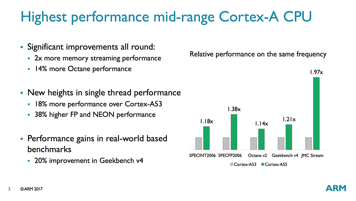
Predictably then, the focus for A55 was on improving performance. The A53’s dual-issue, in-order core, which serves as the starting point for A55, already delivers good throughput, so ARM focused on improving the memory system. A new data prefetcher, an integrated L2 cache that reduces latency by 50%, and an extra level of L3 cache (among other changes) give the A55 significantly better memory performance—quantified by a nearly 2x improvement in the LMBench memory copy test. The numbers provided by ARM also show an 18% performance gain in SPECint 2006 and an even bigger 38% gain in SPECfp 2006 relative to the A53. These numbers, as well as the others shown in the chart, comparing the A55 and A53 are at the same frequency, same L1/L2 cache sizes, same compiler, etc. and are meant to be a fair comparison. The actual gains should actually be a little higher, because partner SoCs will benefit from adding the L3 cache, which these numbers do not include.
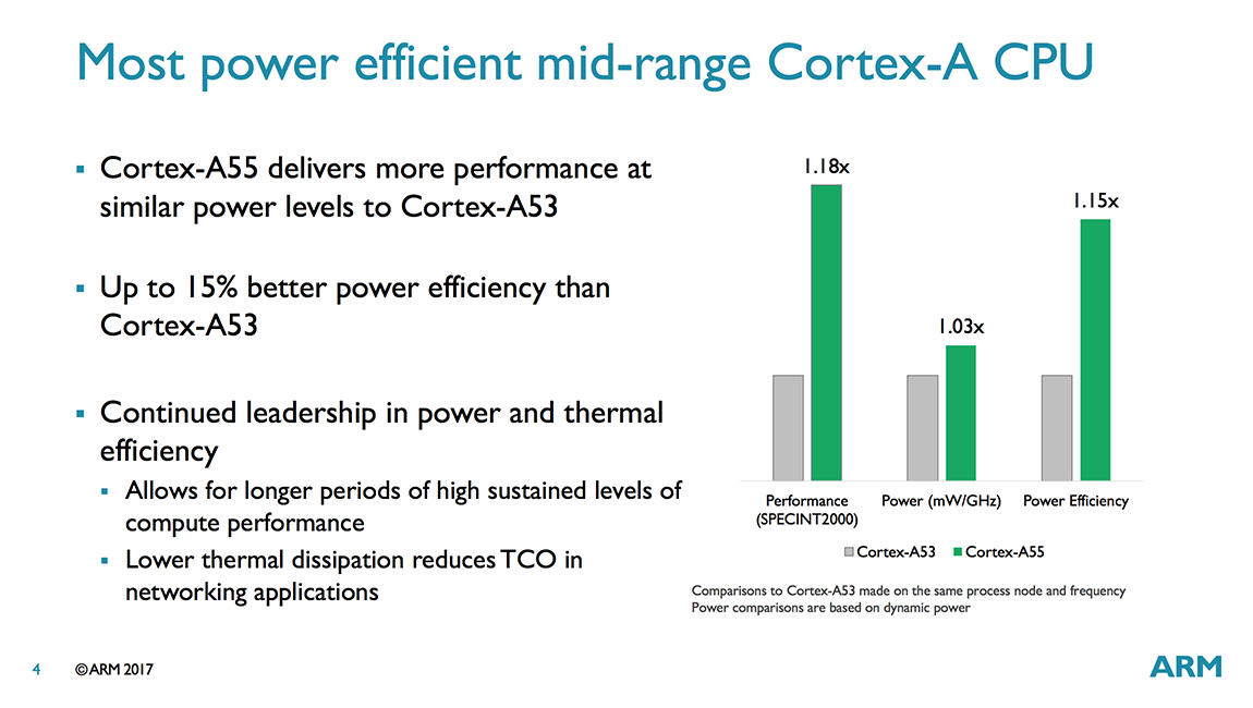
The additional performance does not come for free, however. Power consumption is up 3% relative to the A53 (iso-process, iso-frequency), but power efficiency still improves by 15% when running SPECint 2000 because of its higher performance.
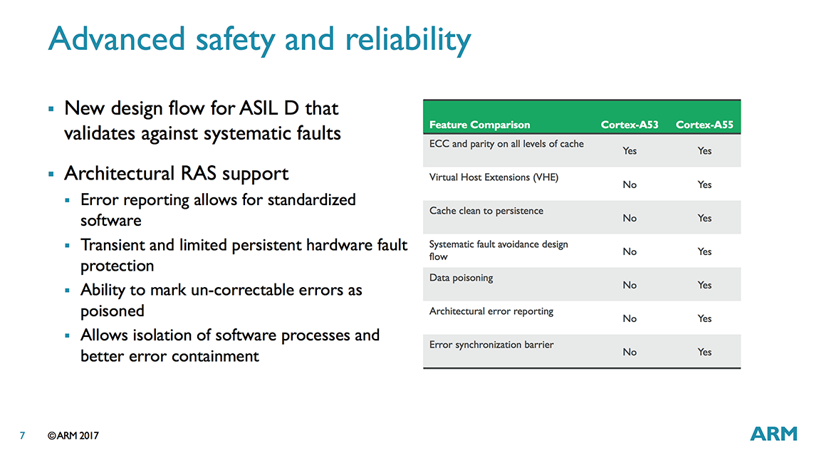
The A55 includes several new features too that will help it expand into new markets. Virtual Host Extensions (VHE) are very important for the automotive market and the advanced safety and reliability features, including architectural RAS support and ECC/parity for all levels of cache are critical for many applications, including automotive and industrial. There’s new features for infrastructure applications too, including a new Int8 dot product instruction (useful for accelerating neural networks). Because A55 is compatible with DynamIQ, it also gets cache stashing and access to a 256-bit AMBA 5 CHI port.
When ARM announced the A73 last year, it talked a lot about improving sustained performance and working within a tight thermal envelope. In other words, the A73 was all about improving power efficiency. The A75 goes in a different direction: Taking advantage of the A73’s thermal headroom, ARM focused on improving performance while maintaining the same efficiency as the A73.
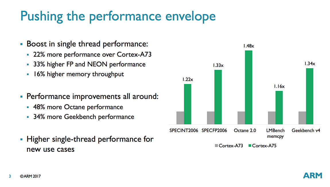
Our previous performance testing revealed mixed results when comparing the A73 to the A72—not too surprising given the significant differences in microarchitecture—with the A73 generally outpacing the A72 by a small margin for integer tasks but falling behind the older CPU in floating point workloads. Things look better for the A75, at least based on ARM’s numbers, which show noticeable gains over the A73 in both integer and floating-point workloads as well as memory streaming.
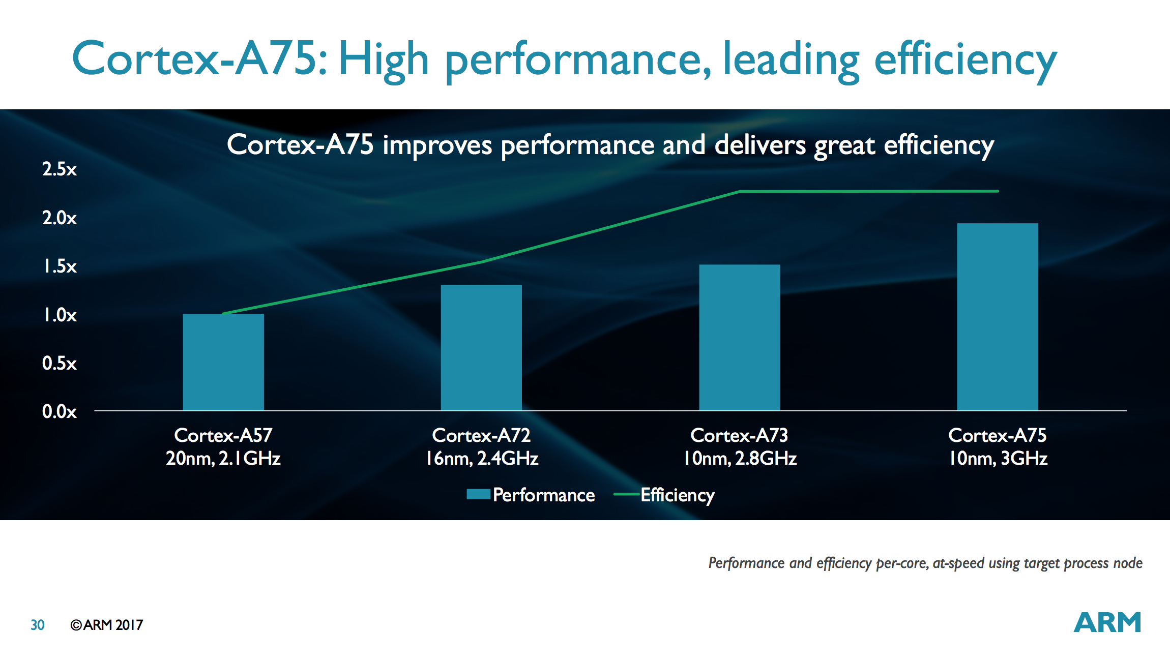
The graph above shows that the A75 operating at 3GHz on a 10nm node achieves better performance and the same efficiency as an A73 operating at 2.8GHz on a 10nm node, which means the A75 consumes more power. How much more is difficult to tell based on this one simple graph. We know that the A73 is thermally limited when using 4 cores (albeit less so than the A72), so the A75 definitely will be as well. This is not a common scenario, however. Most mobile workloads only fire up 1-2 cores at a time and usually only in short bursts. ARM obviously felt comfortable enough using the A73’s extra thermal headroom to boost performance without negatively impacting sustained performance.
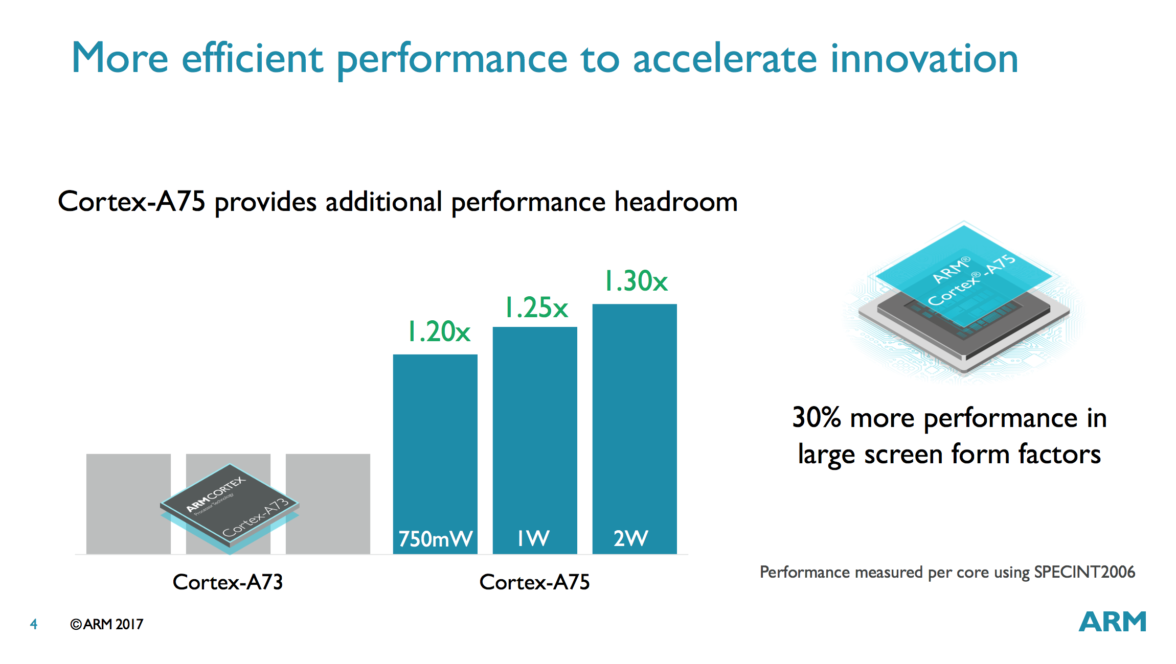
ARM wants to push the A75 into larger form-factor devices with power budgets beyond mobile’s 750mW/core too by pushing frequency higher. Something like a Chromebook or a 2-in-1 ultraportable come to mind. At 1W/core the A75 delivers 25% higher performance than the A73 and at 2W/core the A75’s advantage bumps up to 30% when running SPECint 2006. If anything, these numbers highlight why it’s not a good idea to push performance with frequency alone, as dynamic power scales exponentially.
ARM targeted the A73 specifically at mobile by focusing on power efficiency and removing some features useful for other applications to simplify the design, including no ECC on the L1 cache and no option for a 256-bit AMBA 5 CHI port. With A75, there’s now a clear upgrade path from A72. For the server and infrastructure markets, A75 supports ECC/parity for all levels of cache and AMBA 5 CHI for connecting to larger CCI, CCN, or CMN fabrics, and for automotive and other safety critical applications there’s architectural RAS support, protection against data poisoning, and improved error management.
On the next few pages, we’ll dive deeper into the technical details and features of ARM’s new IP, including DynamIQ (the next iteration of big.LITTLE), Cortex-A75, and Cortex-A55.


104 Comments
View All Comments
alpha64 - Monday, May 29, 2017 - link
Or, perhaps, is this talking about Max and Min configurations of the DSU itself, and not the core (which is not clear in the sentence either)?jjj - Monday, May 29, 2017 - link
Got to be DSU max and min but can't be with the L3$ as 4MB L3$ is huge.hMunster - Monday, May 29, 2017 - link
In what mobile usage scenario is having 7 small cores and 1 big one an advantage over having just 3 small cores and 1 big one?Meteor2 - Monday, May 29, 2017 - link
Are you trolling...?Actual answer: Android is always doing loads of things at once which don't need doing particularly quickly (I.e. aren't at the direct behest of the user), but do need doing efficiently. The throughput needed is more than three small cores can provide.
aryonoco - Monday, May 29, 2017 - link
This website has itself proven that Android does use 8 cores and these extra cores do bring improvements in overall experience.Personally, I'm hopeful that SoC vendors actually do following ARM here and kill off 8 little cores in favour of a 1+7 design. Would translate into a huge single threaded improvement for end users.
Eden-K121D - Monday, May 29, 2017 - link
Better to have 2 + 6 or even 2+4phoenix_rizzen - Monday, May 29, 2017 - link
Yeah, a 2+6 A75/55 arrangement would be neat to see. 4+4 seems like overkill in a phone, but could be useful in a high-res tablet or Chromebook.Wonder what the TDP would be for an 8-core cluster of just A75s. :) Chromebook or laptop?
aryonoco - Monday, May 29, 2017 - link
Well ARM says the TDP of A75 is from 750mW per core to 2W per core based on clock speed. Obviously an SoC has other components as well, and cache and the interconnects use power as well, not to mention the GPU. So depending on how you clock it and how much cache it has and what GPU it has, I'd say that an 8-core A75 SoC on 10nm process would have a TDP of somewhere between 12W to 25W.And as much as I'd like to see such a 8-Core A75 SoC, this is pure fantasy. The volume of Chromebooks is too low to design bespoke SoCs for them, they'll be just use whatever is designed for phones.
aryonoco - Monday, May 29, 2017 - link
Sure, I would prefer a 2+4 to a 1+7 configuration as well. I've always thought that 2+4 is the sweet spot for big.LITTLE.But 2+4 is going to be a lot bigger than 1+7. These LITTLE cores are extremely tiny, the A53 is about 1mm on 16nm fab process. Which is why the mid-range of the market has gone for 8-core A53s in the last couple of years.
2+4 is a lot bigger so it's not even a consideration for this end of the market. 2+4 could have been done with big.LITTLE but the fact that there were so few 2+4 SoCs tells you that the market just didn't think it was worth it. 1+7 on the other hand was not possible with big.LITTLE, but is possible with DynamIQ, and according to ARM is only a little bigger than 8 small cores, so I'm hoping that the market sees value in that for the midrange.
0iron - Monday, May 29, 2017 - link
But die size will be bigger. The reason why ARM introduce 1+7 is because die size is 13% bigger than 8xA53 while 8xA55 is 10% more. So, it's only 3% more area than 8xA55 but provide 2x single core performance.